

Pixel structure and display panel
A pixel structure and pixel electrode technology, applied in nonlinear optics, instruments, optics, etc., can solve problems such as inconsistency, misdirection, and dark lines of liquid crystals, and achieve the effect of improving dark lines and increasing transmittance
- Summary
- Abstract
- Description
- Claims
- Application Information
AI Technical Summary
Problems solved by technology
Method used
Image

Examples
Embodiment Construction
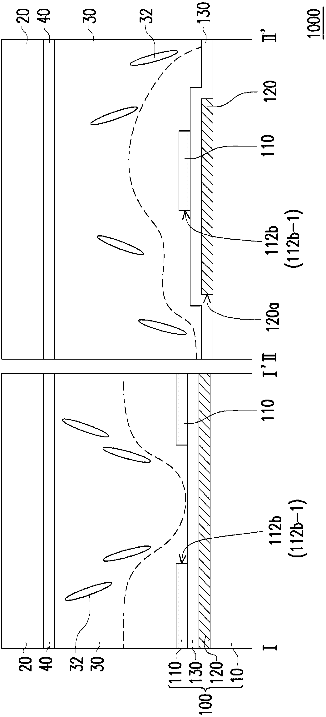
[0067] figure 1 It is a partial cross-sectional schematic diagram of a display panel according to an embodiment of the present invention. Please refer to figure 1 , the display panel 1000 includes a pixel structure 100 , a second substrate 20 and a liquid crystal layer 30 . The second substrate 20 is opposite to the first substrate 10 of the pixel structure 100 . The liquid crystal layer 30 is disposed between the first substrate 10 and the second substrate 20 . In this embodiment, the display panel 1000 may further include a second electrode 40 . The potential voltage difference between the second electrode 40 and the pixel electrode 110 is used to drive the liquid crystal molecules 32 , thereby enabling the display panel 1000 to display images. In this embodiment, the second electrode 40 can be selectively disposed on the second substrate 20, and is located between the second substrate 20 and the liquid crystal layer 30, and the display panel 1000 can be regarded as a mu...
PUM
 Abstract
Description
Claims
Application Information