Double patterning method

A double patterning and planarization technology, applied in the direction of electrical components, semiconductor/solid-state device manufacturing, circuits, etc., can solve the problems of poor target graphics quality, affecting the performance and yield of semiconductor structures, etc., to achieve small surface height difference and improve quality effect

Active Publication Date: 2018-03-09
SEMICON MFG INT (SHANGHAI) CORP +1
View PDF6 Cites 2 Cited by
  • Summary
  • Abstract
  • Description
  • Claims
  • Application Information

AI Technical Summary

Problems solved by technology

[0004] However, in the prior art, the double patterning method is used to etch the substrate, and the quality of the target pattern formed in the substrate after etching is poor, which affects the performance and yield of the formed semiconductor structure

Method used


Image

  • Double patterning method
  • Double patterning method
  • Double patterning method

Examples


Embodiment Construction

[0032] It can be known from the background art that, in the prior art, the double patterning method is used to etch the substrate, and the quality of the pattern formed in the etched substrate is poor.

[0033] Figure 1 to Figure 5 It is a schematic cross-sectional structure diagram of the process of forming a semiconductor structure using a double patterning method.

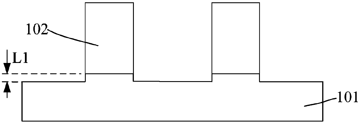
[0034] reference figure 1 , A substrate 101 is provided, and a plurality of discrete core layers 102 are formed on the surface of the substrate 101.

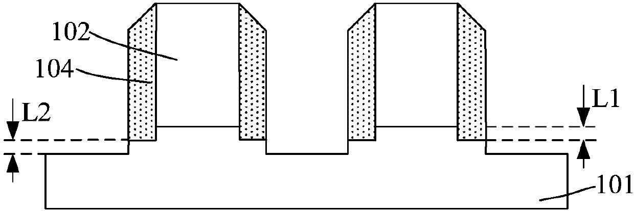
[0035] Moreover, the process of forming the core layer 102 is likely to cause over etch to the substrate 101, so that the top surface of the substrate 101 under the core layer 102 is higher than the top surface of the substrate 101 exposed by the core layer 102, and the top surface of the substrate 101 under the core layer 102 The minimum distance between the top of the substrate 101 and the top of the substrate 101 exposed by the core layer 102 is L1.

[0036] reference...


PUM


Abstract

The invention discloses a double patterning method. The method comprises steps: lateral wall layers are formed on the top part and the side wall of a core layer and the substrate in a second area; a sacrificial layer is formed on the lateral wall layer in a second sub area; the top part of the sacrificial layer and the top part of the lateral wall layer are subjected to planarization processing toexpose the top part of the core layer; a first etching process is adopted to etch the sacrificial layer and the core layer, and thus, the top part of the remaining core layer is flush with the top part of the remaining sacrificial layer in the second sub area; a second etching process is adopted to etch and remove the remaining core layer, the lateral wall layer in the second sub area is also etched and removed, and the first area substrate and the second sub area substrate are exposed; and with the lateral wall layer in a first sub area as a mask, the substrate is etched to form a target pattern. The surface height difference between the remaining substrates at two sides of the target pattern can be reduced, and the formed target pattern quality is improved.

Description

Technical field [0001] The present invention relates to the technical field of semiconductor manufacturing, in particular to a method of double patterning. Background technique [0002] Driven by Moore's Law, semiconductor technology continues to move towards smaller process nodes. With the continuous advancement of semiconductor technology, the functions of devices continue to be powerful, but the difficulty of semiconductor manufacturing is increasing day by day. Lithography is the most critical production technology in the semiconductor manufacturing process. With the continuous reduction of semiconductor process nodes, the existing light source lithography technology can no longer meet the needs of semiconductor manufacturing. Ultra-ultraviolet lithography (EUV), Multi-beam maskless technology and nanoimprint technology have become the research hotspots of next-generation lithography candidate technologies. However, the above-mentioned next-generation lithography candidate ...

Claims


Application Information

Patent Timeline
Patent Type & Authority Applications(China)
IPC IPC(8): H01L21/308
CPCH01L21/3083H01L21/3086
Inventor 王彦张城龙张海洋
Owner SEMICON MFG INT (SHANGHAI) CORP
Why Eureka
Try Eureka