Supercharge Your Innovation With Domain-Expert AI Agents!

Graphene pellicle for extreme ultraviolet lithography

A graphene layer and material layer technology, applied in the field of graphene layer formation, can solve the problems of diaphragm deformation, difficulty in manufacturing effective thin films on a large scale, short wavelength, etc.

Inactive Publication Date: 2018-03-13
TAIWAN SEMICON MFG CO LTD
View PDF0 Cites 0 Cited by
  • Summary
  • Abstract
  • Description
  • Claims
  • Application Information

AI Technical Summary

Problems solved by technology

[0003] Unlike masks used in deep-UV lithography, which traditionally employ thin films to protect the mask surface, it is currently difficult to fabricate effective thin films for EUV masks on a large scale
One reason is that the wavelength of EUV radiation is very short and the membrane of a conventional film will absorb it so much that the membrane will deform from overheating after a few uses and will also substantially reduce the reach of the target. extreme ultraviolet energy

Method used

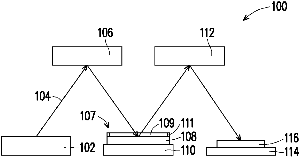
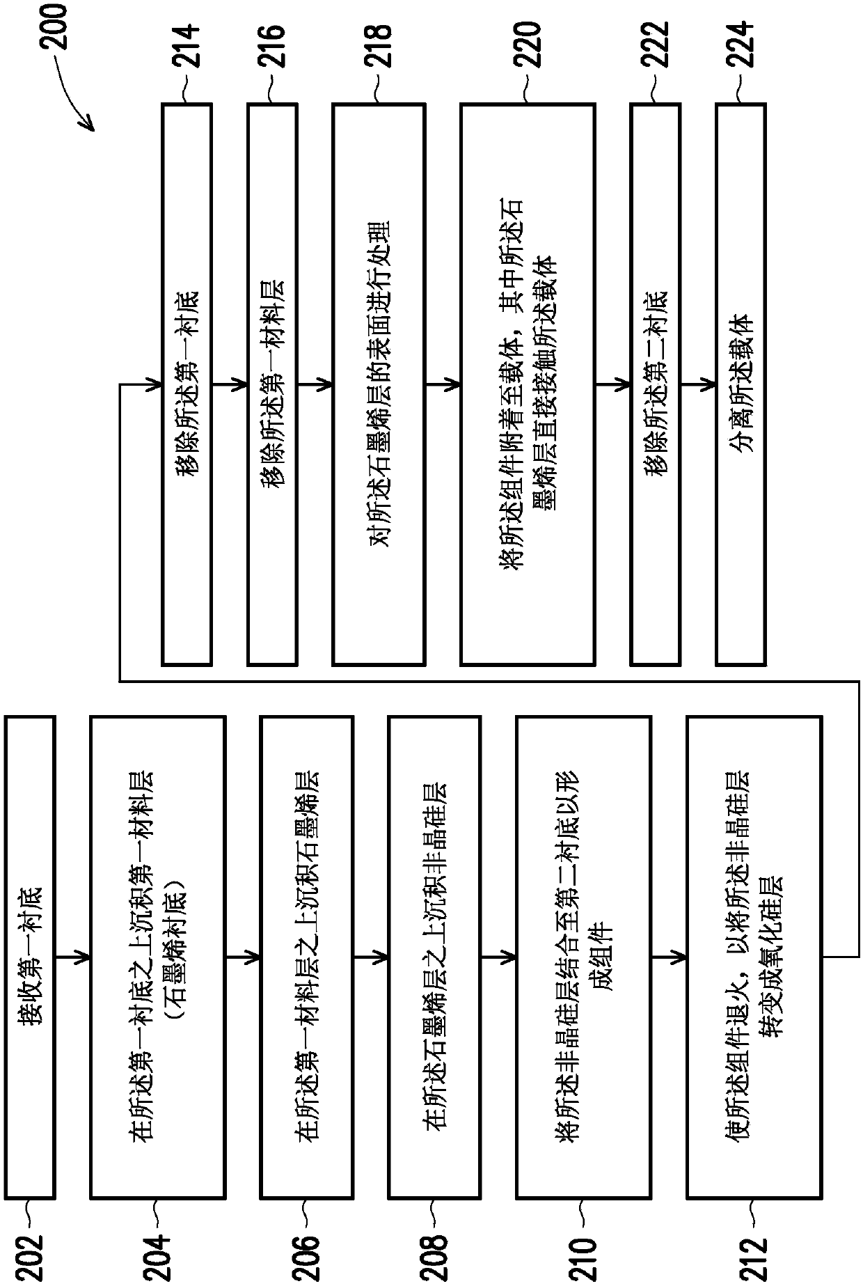

Image

  • Graphene pellicle for extreme ultraviolet lithography
  • Graphene pellicle for extreme ultraviolet lithography
  • Graphene pellicle for extreme ultraviolet lithography

Examples


Embodiment Construction

[0035] The following disclosure provides many different embodiments, or examples, for implementing different features of the presented subject matter. Specific examples of components and arrangements are set forth below to simplify the present disclosure. These specific examples are, of course, examples only, and are not intended to be limiting. For example, in the following description, forming a first feature "on" a second feature or "on" a second feature may include embodiments in which the first and second features are formed in direct contact, and may also include embodiments in which Embodiments in which an additional feature may be formed between the first feature and the second feature such that the first feature and the second feature may not be in direct contact. Additionally, this disclosure may repeat reference numbers and / or letters in various instances. This repetition is for the purposes of brevity and clarity and does not in itself indicate a relationship bet...


PUM


Abstract

The invention discloses a graphene layer formation method. The graphene layer formation method comprises steps of depositing a first material layer over a first substrate and depositing a graphene layer over the first material layer. The method further includes steps of depositing an amorphous silicon layer over the graphene layer and bonding the amorphous silicon layer to a second substrate, thereby forming an assembly. The geaphene layer formation method further includes asteps of annealing the assembly, thereby converting the amorphous silicon layer to a silicon oxide layer. The method further includes steps of removing the first substrate from the assembly and removing the first material layer from the assembly, thereby exposing the graphene layer.

Description

technical field [0001] Embodiments of the present invention relate to a method for forming a graphene layer. Background technique [0002] As the semiconductor industry has progressed to nanotechnology in pursuit of higher device density, higher performance, and lower cost, more stringent requirements have been placed on lithography tools used in semiconductor manufacturing. Technologies such as extreme ultraviolet (EUV) lithography have been utilized to support the critical dimension (CD) requirement of smaller integrated circuit (IC) devices. EUV lithography uses radiation in the EUV region with a wavelength of about 1 nm to 100 nm (eg, 13.5 nm), which is faster than that used in deep ultraviolet (DUV) lithography (eg, 193 nm lithography). The wavelength is much shorter. EUV lithography uses a mask (or reticle) that reflects EUV radiation from a radiation source toward a target, such as a silicon wafer, thereby transferring a pattern from the mask to the target. Any imp...

Claims


Application Information

Patent Timeline
IPC IPC(8): G03F1/62
CPCG03F1/62
Inventor 涂志强陈俊郎蔡嘉雄游秋山张宗裕林志诚刘丙寅李信昌林云跃
Owner TAIWAN SEMICON MFG CO LTD
Features
  • R&D
  • Intellectual Property
  • Life Sciences
  • Materials
  • Tech Scout
  • Unparalleled Data Quality
  • Higher Quality Content
  • 60% Fewer Hallucinations
Learn More