Manufacturing method of array substrate

A manufacturing method and array substrate technology, applied in semiconductor/solid-state device manufacturing, optics, instruments, etc., can solve problems such as short circuit of signal lines, reduction of adhesion between TFT substrate and CF substrate, poor display, etc., and achieve small slope angle, good exposure effect

Inactive Publication Date: 2018-03-13
WUHAN CHINA STAR OPTOELECTRONICS TECH CO LTD
View PDF3 Cites 4 Cited by
  • Summary
  • Abstract
  • Description
  • Claims
  • Application Information

AI Technical Summary

Problems solved by technology

However, reducing the width of the sealant of the liquid crystal display panel will reduce the adhesion between the TFT substrate and the CF substrate. Usually, a groove is dug on the flat layer (PLN) around the TFT substrate so that the contact between the sealant and the TFT substrate The area will not be reduced, but this brings a technical problem. The groove of PLN is generally a deep groove above 1.5 μm, and the slope angle (Taper) of the edge of the groove is very large, generally greater than 50 In the subsequent formation of the pixel electrode (the material of the pixel electrode includes but is not limited to indium tin oxide), there is usually a large amount of residue in the groove, and the remaining material will cause a short circuit between the signal lines, resulting in poor display

Method used


Image

  • Manufacturing method of array substrate
  • Manufacturing method of array substrate
  • Manufacturing method of array substrate

Examples


Embodiment Construction

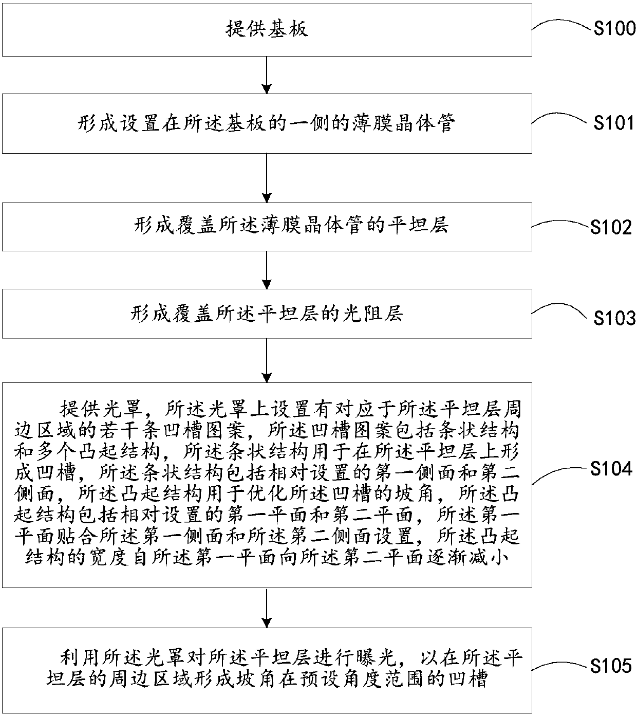
[0021] The following will clearly and completely describe the technical solutions in the embodiments of the present invention with reference to the drawings in the embodiments of the present invention. Apparently, the described embodiments are some, not all, embodiments of the present invention. Based on the embodiments of the present invention, all other embodiments obtained by persons of ordinary skill in the art without making creative efforts shall fall within the protection scope of the present invention.

[0022] Reference herein to an "embodiment" means that a particular feature, structure, or characteristic described in connection with the embodiment can be included in at least one embodiment of the present invention. The occurrences of this phrase in various places in the specification are not necessarily all referring to the same embodiment, nor are separate or alternative embodiments mutually exclusive of other embodiments. It is understood explicitly and implicitl...


PUM

PropertyMeasurementUnit
thicknessaaaaaaaaaa

Abstract

The present invention provides a manufacturing method of an array substrate. The manufacturing method of the array substrate comprises the following steps: providing a substrate; forming a thin film transistor arranged on one side of the substrate; forming a flat layer covering the thin film transistor; forming a photoresist layer covering the flat layer; providing a light cover, wherein the lightcover is provided with a plurality of groove patterns corresponding to the peripheral area of the flat layer, the groove patterns comprises a strip-shaped structure and multiple protruding structures, the strip-shaped structure is used for forming grooves on the flat layer, the strip-shaped structure comprises a first side and a second side opposite to each other, the protruding structures are used for optimizing slope angles of the grooves, each protruding structure comprises a first plane and a second plane opposite to each other, the first planes are arranged on the first side and the second side, and the width of each protruding structure gradually decreases from the first plane to the second plane; exposing the flat layer by using the light cover to form the grooves on the peripheralarea of the flat layer, wherein the slope angles of the grooves are in the range of preset angles. The method can contribute to reducing the slope angles of the grooves on the flat layer.

Description

technical field [0001] The present invention relates to the field of display technology, in particular to a method for manufacturing an array substrate. Background technique [0002] Usually, the liquid crystal display panel is composed of a color filter (Color Filter, CF) substrate, a thin film transistor (Thin Film Transistor, TFT) substrate, a liquid crystal (Liquid Crystal, LC) sandwiched between the color filter substrate and the thin film transistor substrate, and a sealant frame (Sealant). . In order to solve the problem that the brightness of the real screen remains unchanged and the power consumption of the backlight brightness does not increase, technicians have come up with various methods to increase the transmittance. Now the conventional method is to use a flat layer to reduce the number of pixel electrodes and common electrodes and signal lines or The capacitance between scanning lines, generally, the thickness of the flat layer is more than 1.5 μm, which inc...

Claims


Application Information

Patent Timeline
Patent Type & Authority Applications(China)
IPC IPC(8): H01L21/84G02F1/1333
Inventor 王丽
Owner WUHAN CHINA STAR OPTOELECTRONICS TECH CO LTD
Why Eureka
Try Eureka