A method of manufacturing a carrier board

A manufacturing method and carrier board technology, which are used in chemical/electrolytic methods to remove conductive materials, multi-layer circuit manufacturing, circuit substrate materials, etc. Small thermal expansion coefficient and good dimensional stability

Active Publication Date: 2021-01-08
通元科技(惠州)有限公司
View PDF3 Cites 0 Cited by
  • Summary
  • Abstract
  • Description
  • Claims
  • Application Information

AI Technical Summary

Problems solved by technology

[0003] At present, the HDI circuit boards used in mobile phones have reached the limit of active and passive components, and more and more functions are wanted to be packed in a mobile phone. Battery, the battery has become the biggest shortcoming of current electronic technology. Therefore, design engineers have turned their brains to the PCB and started to make the PCB for mobile phones extremely thin. However, how to make the PCB extremely thin is the biggest problem at present.

Method used


Image

  • A method of manufacturing a carrier board

Examples


Embodiment Construction

[0026] In order to enable those skilled in the art to better understand the technical solution of the present invention, the product of the present invention will be further described in detail below in conjunction with examples and accompanying drawings.

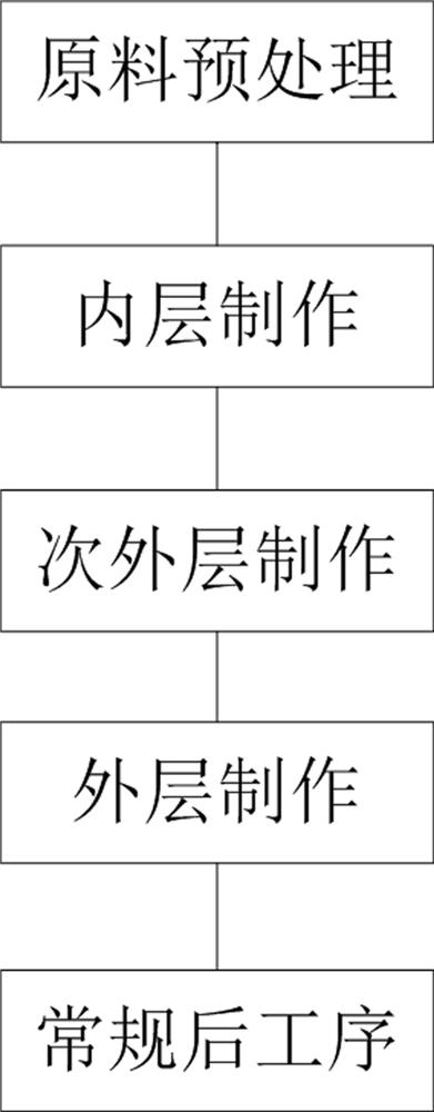
[0027] Such as figure 1 As shown, a manufacturing method of a kind of carrier board includes the following steps,

[0028] The first step is raw material pretreatment. First, the core board is made of BT material, and the upper and lower surfaces of the core board are

[0029] Coated with a copper layer to make the core board form a copper-clad BT core board, then cut the copper-clad BT core board according to the required size, and clean the board surface of the cut copper-clad BT core board;

[0030] The second step is the production of the inner layer. The inner layer production includes sequentially performing copper reduction, browning, laser blind holes, glue removal, hole metallization, hole filling electroplating, ...


PUM


Abstract

The invention discloses a manufacturing method of a substrate-like PCB. The manufacturing method comprises the following steps of raw material pretreatment: firstly a core board is manufactured by using BT material, a copper layer is coated on the upper and lower surfaces of the core board and the core board is enabled to form a copper-clad BT core board, then the copper-clad BT core board is cutaccording to the required side and board surface cleaning treatment is performed on the cut copper-clad BT core board; internal layer manufacturing, second external layer manufacturing and external layer manufacturing: concretely, internal layer manufacturing includes the process of performing copper reduction, brownification, blind hole lasering, adhesive dispensing, hole metallization, hole filling and electroplating, line manufacturing and pressing on the pretreated BT core plate; and routine post-treatment which is performed after completion of internal and external layer manufacturing. The manufacturing method of the substrate-like PCB has the advantages of being narrow in linewidth so as to further meet the SIP packaging technical requirements.

Description

technical field [0001] The invention relates to the technical field of manufacturing printed circuit boards, in particular to a method for manufacturing a carrier board. Background technique [0002] "Substrate-Like PCB" is called Substrate-Like PCB in English, or SLP for short. This "substrate-like PCB" is based on existing HDI technology and is similar to an IC substrate, but it is not as high as an IC substrate. This kind of "substrate-like PCB" will have higher precision than traditional HDI, but it is still used to carry various active components, not IC substrates used in semiconductor packaging. [0003] At present, the HDI circuit boards used in mobile phones have reached the limit of active and passive components, and more and more functions are wanted to be packed in a mobile phone. Battery, the battery has become the biggest shortcoming of current electronic technology. Therefore, design engineers have turned their brains to the PCB and started to make the PCB f...

Claims


Application Information

Patent Timeline
Patent Type & Authority Patents(China)
IPC IPC(8): H05K3/46H05K3/06H05K1/03
CPCH05K1/0353H05K3/06H05K3/4602H05K3/4644H05K2203/052
Inventor 陈志宇乔鹏程赵宏静
Owner 通元科技(惠州)有限公司
Why Eureka
Try Eureka