
Flexible display panel and preparation method thereof

A flexible display and panel technology, applied in semiconductor/solid-state device manufacturing, electrical components, electric solid-state devices, etc., can solve problems such as glass and polyimide film adhesion, to avoid inseparability, reduce design distance, prevent Effects of ACF Spillover

Inactive Publication Date: 2018-03-20
WUHAN CHINA STAR OPTOELECTRONICS TECH CO LTD
View PDF5 Cites 33 Cited by
  • Summary
  • Abstract
  • Description
  • Claims
  • Application Information

AI Technical Summary

Problems solved by technology

[0004] In order to solve the above problems, the present invention provides a flexible display panel for preventing ACF glue overflow and its preparation method, thereby solving the problem of glass and polyimide film adhesion caused by ACF glue overflow phenomenon

Method used


Image

  • Flexible display panel and preparation method thereof
  • Flexible display panel and preparation method thereof
  • Flexible display panel and preparation method thereof

Examples


Embodiment Construction

[0026] The following description is a preferred embodiment of the present invention, it should be pointed out that for those skilled in the art, without departing from the principle of the present invention, some improvements and modifications can also be made, and these improvements and modifications are also considered Be the protection scope of the present invention.

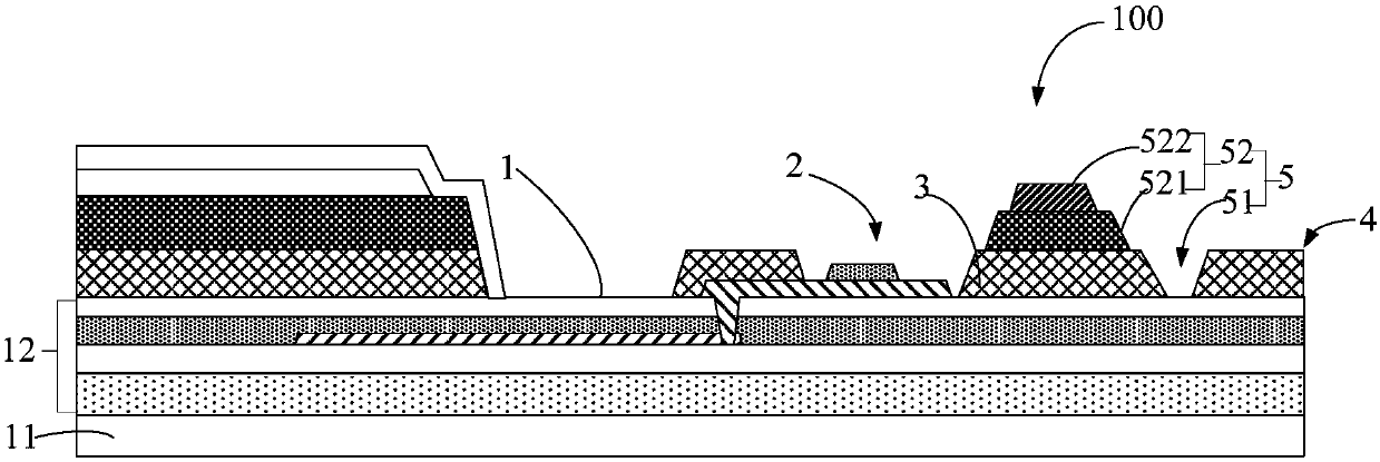
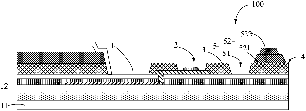
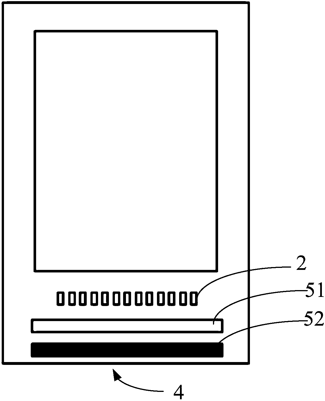
[0027] Such as figure 1 and figure 2 As shown, the embodiment of the present invention provides a flexible display panel 100, the flexible display panel 100 is divided into a display area (not shown in the figure) and a non-display area 1, the non-display area 1 includes a substrate 11, a set The insulating layer 12 on the substrate, the planar layer 3 (PLN) arranged on the insulating layer, the chip bonding region 2 and the outer edge 4 arranged on the planar layer 3, the chip bonding region 2 and An ACF glue overflow blocking portion 5 is formed between the outer edges 4 , and the ACF glue overflow block...


PUM

PropertyMeasurementUnit
Thicknessaaaaaaaaaa

Abstract

The present invention provides a flexible display panel. The flexible display panel comprises a display area and a non-display area. The non-display area comprises a substrate, an insulation layer arranged on the substrate, a planarization layer arranged on the insulation layer, a chip bonding area arranged on the planarization layer and an outer edge. An ACF (Anisotropic Conductive Film) excessive glue blocking portion is formed between the chip bonding area and the outer edge, and the ACF excessive glue blocking portion is extended along the extension direction of the outer edge. The ACF excessive glue blocking portion can avoid ACF overflowing to avoid a phenomenon that glass and a polyimide film cannot be separated. The present invention further provides a preparation method of a flexible display panel. The method comprise the steps of: providing the display substrate, wherein the display substrate comprises a plurality of panel areas, each panel area comprises a display area and anon-display area, and each non-display area comprises the substrate, the insulation layer, the planarization layer, the chip bonding area and a cutting area; forming the ACF excessive glue blocking portion at a position between the chip bonding area and the cutting area through adoption of patterning processing; and cutting the display substrate along the cutting area, and obtaining the flexibledisplay panel.

Description

technical field [0001] The invention relates to the field of flexible display panels, in particular to a flexible display panel for preventing ACF glue overflow and a preparation method thereof. Background technique [0002] ACF (Anisotropic Conductive Film) is a conductive adhesive used on the display panel of an active matrix organic light-emitting diode (AMOLED) to bond the chip to the display panel. To the role of up and down conduction. [0003] For flexible low-temperature polysilicon AMOLED (LTPS-AMOLED), the manufacturing process is to first coat polyimide film on the glass, and then perform low-temperature polysilicon (LTPS) process on the polyimide film, in electroluminescence (EL) After the process is completed, dicing and chip bonding are performed, and the laser lift-off (LLO) process is performed to separate the glass and the polyimide film. However, due to the problem of glue overflow in ACF in flexible LTPS-AMOLED, after cutting, the overflow glue produced ...

Claims


Application Information

Patent Timeline
IPC IPC(8): H01L27/32H01L51/52H01L51/56
CPCH10K59/122H10K59/121H10K50/84H10K71/00
Inventor 陈彩琴
Owner WUHAN CHINA STAR OPTOELECTRONICS TECH CO LTD
Learn More