improved power mos
A device and semiconductor technology, applied in the field of semiconductor devices, can solve problems such as reducing the width of the embedded gate
- Summary
- Abstract
- Description
- Claims
- Application Information
AI Technical Summary
Problems solved by technology
Method used
Image


Examples
Embodiment Construction
[0014] Many well-known manufacturing steps, components, and connectors have been omitted or not described in detail in the specification so as not to obscure the present disclosure.
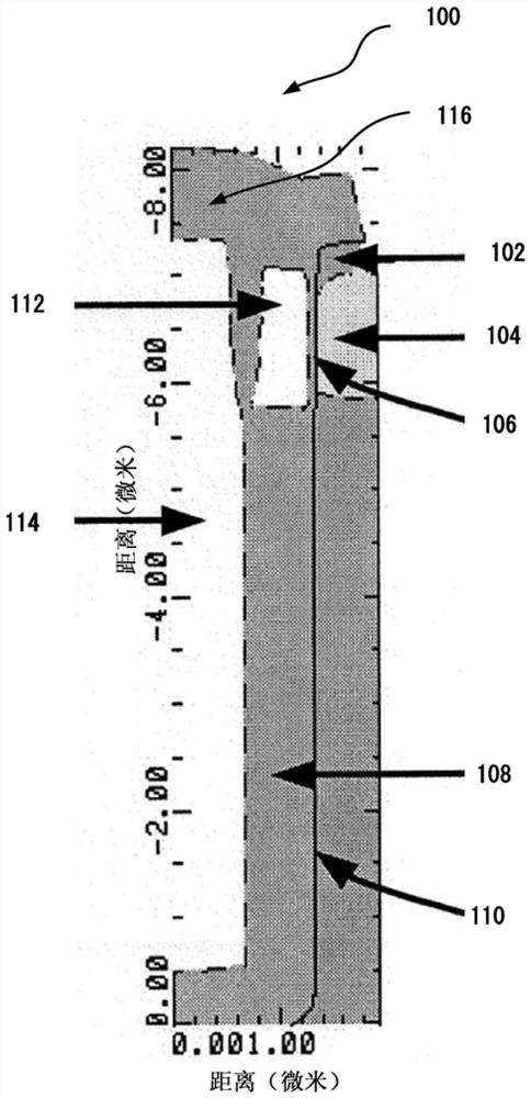
[0015] figure 1 A schematic diagram depicting a cross-sectional view of a device 100 fabricated using a process described later in this document. The device 100 includes a gate electrode 112 , a RESURF plate 114 , a source region 102 , a body region 104 , a gate dielectric 106 , and a trench 110 filled with a dielectric 108 .
[0016] One way to fabricate such a device is to fabricate the gate electrode in a shallow trench and then create a RESURF plate by implanting the p-type RESURF region with high energy to make the RESURF plate deeper (to achieve a high breakdown voltage (BV dss )). However, as the energy is increased, the implanted species will infiltrate the implant mask, which is placed in place to protect areas other than the area through which the RESURF plate is created. This penetr...
PUM
 Abstract
Description
Claims
Application Information
 - R&D
- Intellectual Property
- Life Sciences
- Materials
- Tech Scout
- Unparalleled Data Quality
- Higher Quality Content
- 60% Fewer Hallucinations
Browse by: Latest US Patents, China's latest patents, Technical Efficacy Thesaurus, Application Domain, Technology Topic, Popular Technical Reports.
© 2025 PatSnap. All rights reserved.Legal|Privacy policy|Modern Slavery Act Transparency Statement|Sitemap|About US| Contact US: help@patsnap.com