non-volatile semiconductor storage device

A storage device, non-volatile technology, used in information storage, memory systems, static memory, etc.

Active Publication Date: 2020-06-30
WINBOND ELECTRONICS CORP
View PDF9 Cites 0 Cited by
  • Summary
  • Abstract
  • Description
  • Claims
  • Application Information

AI Technical Summary

Problems solved by technology

[0014] The object of the present invention is to solve such problems and provide a nonvolatile semiconductor memory device equipped with a chip-level ECC function that can achieve miniaturization and high speed.

Method used


Image

  • non-volatile semiconductor storage device
  • non-volatile semiconductor storage device
  • non-volatile semiconductor storage device

Examples


Embodiment

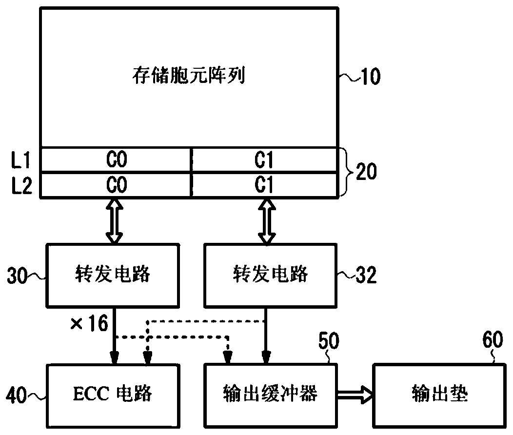
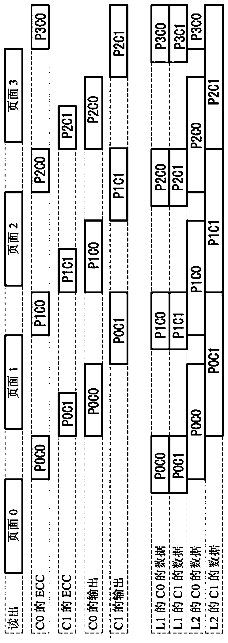
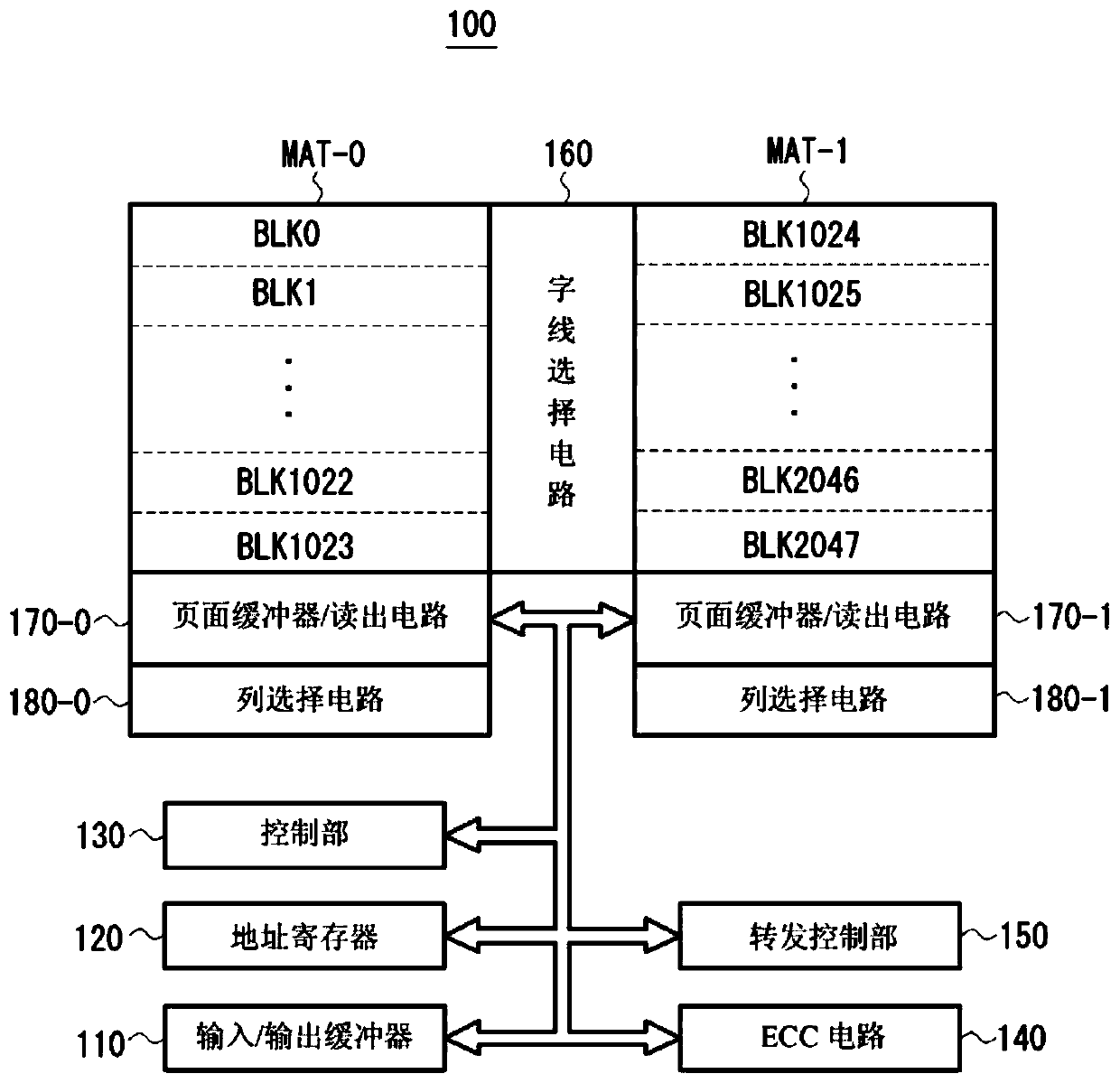
[0057] image 3 It is a block diagram showing a configuration example of a NAND flash memory according to an embodiment of the present invention. as it should image 3As shown, the flash memory 100 includes: a memory cell array 10, including two memory pads MAT-0 and MAT-1 formed with a plurality of memory cells arranged in a matrix; an input / output buffer 110 connected to External input / output terminal I / O; address register (address register) 120, accepts the address data from input / output buffer 110; chip enable (chip enable) CE, command latch enable (command latch enable) CLE, address latch enable (address latch enable) ALE, ready / busy (ready / busy) RY / BY, etc.) to control The actions of reading, programming and erasing; the ECC circuit 140 performs error detection and correction of the data to be programmed to the memory pads MAT-0 and MAT-1 or the data read from them; the forwarding control unit 150 is based on the control unit 130 to control the forwarding of data; the...


PUM


Abstract

The present invention provides a non-volatile semiconductor memory device, comprising: a memory array, including memory pads (MAT-0, MAT-1); a page buffer (170-0), which maintains the The data out; Page buffer (170-1), keeps the data read from storage pad (MAT-1); ECC circuit (140), carries out error detection and correction of data; Output buffer (110), outputs data and a forwarding control section, controlling data forwarding between the page buffer (170-0), the page buffer (170-1), the ECC circuit (140), and the output buffer (110). When the memory mat (MAT-0) is selected, the transfer control unit transfers the data held in the page buffer (170-0) to the page buffer (170-1) of the memory mat (MAT-1).

Description

technical field [0001] The present invention relates to a kind of non-volatile semiconductor memory device, relate in particular to a kind of NAND flash memory (flash memory) equipped with chip level (onchip) error detection and correction (Error Checking Correction, ECC) function Read method. Background technique [0002] Currently on memory chips, redundancy schemes are used to apparently repair physical defects in memory elements generated during the manufacturing process. Furthermore, in addition to physical restoration by redundant memory, there is an error detection and correction circuit as a countermeasure against soft errors. [0003] In the NAND flash memory of Patent Document 1, the cache register is composed of two parts. While outputting data from one of the cache registers, an error correction code operation is performed on the data of the other cache register. The delay of error correction code operation is removed from the output, enabling high-speed readou...

Claims


Application Information

Patent Timeline
Patent Type & Authority Patents(China)
IPC IPC(8): G11C16/06G06F11/10
CPCG06F11/1064G06F11/1068G11C16/06G11C16/0483G11C2029/0411G06F11/1048G06F12/0238G11C16/26G06F3/0608G06F3/064G06F12/0246G06F12/126G11C16/3409G11C29/42G11C29/4401
Inventor 须藤直昭
Owner WINBOND ELECTRONICS CORP
Why Eureka
Try Eureka