Nonvolatile memory for catching charges in isolative films

A non-volatile storage and non-volatile technology, applied in the field of non-volatile semiconductor memory, can solve the problems of delay amplification circuit activation, unable to generate read data at high speed, unable to achieve high-speed access, etc., to achieve high-speed And the effect of accurate reading

Inactive Publication Date: 2008-09-03
MITSUBISHI ELECTRIC CORP
View PDF4 Cites 0 Cited by
  • Summary
  • Abstract
  • Description
  • Claims
  • Application Information

AI Technical Summary

Problems solved by technology

[0042] However, the current flowing through the memory cell MC is on the order of μA. Therefore, in order to accurately read data with a sufficient margin, the time until time t0, that is, the charging time of the capacitive element 921 must be sufficiently long.
In this way, its read data cannot be generated at high speed, resulting in the problem that high-speed access cannot be realized.
[0043] In particular, in the case of selecting a 1-bit memory cell, continuously reading the 2-bit data stored in the 1-bit memory cell internally, and reading it to the outside in parallel, it is impossible to read data at a high speed. The problem with multivalued data like this
[0044] At the time of reading the data, in the configuration in which the capacitive element 921 is precharged to a predetermined voltage level and a current is supplied to the selected bit line according to the charged voltage of the capacitive element 921, similarly, in the programming state and the erasing state, In the memory cell, in order to give a sufficient difference in the charging voltage level of the capacitive element, it is necessary to delay the activation of the amplifier circuit 922, resulting in the same problem

Method used


Image

  • Nonvolatile memory for catching charges in isolative films
  • Nonvolatile memory for catching charges in isolative films
  • Nonvolatile memory for catching charges in isolative films

Examples


Embodiment 1

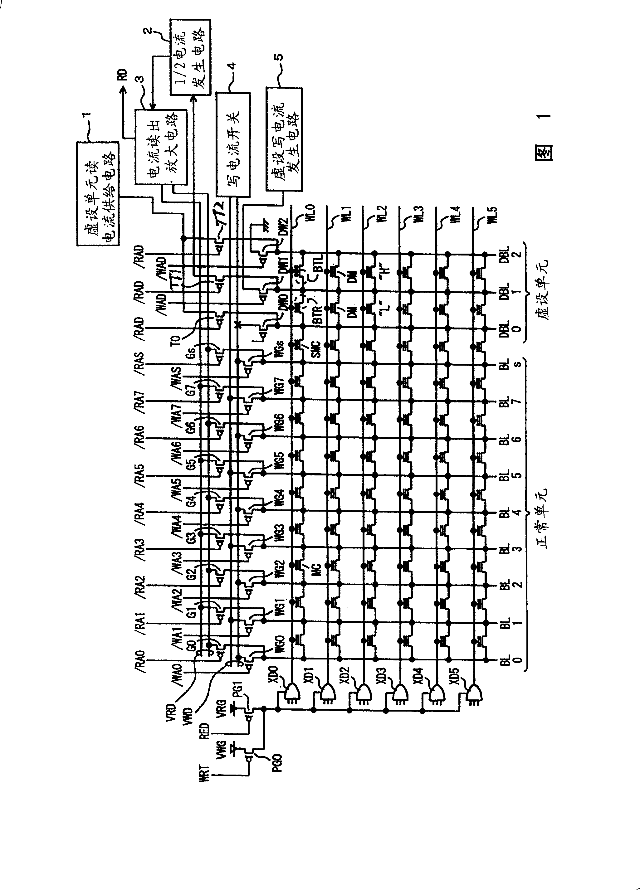
[0107] FIG. 1 is a diagram schematically showing the configuration of important parts of a nonvolatile semiconductor memory according to Embodiment 1 of the present invention. In FIG. 1 , the memory cell array includes normal memory cells (normal cells) MC arranged in rows and columns, and dummy cells DM arranged in line with the normal cells MC in the row direction. Word lines WL are arranged corresponding to each row of normal cells MC and dummy cells DM. In FIG. 1 , six word lines WL0 to WL5 are representatively shown.

[0108] Bit lines BL are arranged corresponding to each column of normal cells MC and shared by memory cells of adjacent columns. In FIG. 1 , normal bit lines BL0 to BL7 are representatively shown. The bit line BLs is arranged adjacent to the bit line BL7. Dummy bit lines DBL are arranged corresponding to each column of dummy cells DM. In FIG. 1, since dummy cells DM are arranged in two columns, three dummy bit lines DBL0 to DBL2 are shown.

[0109] Non-a...

Embodiment 2

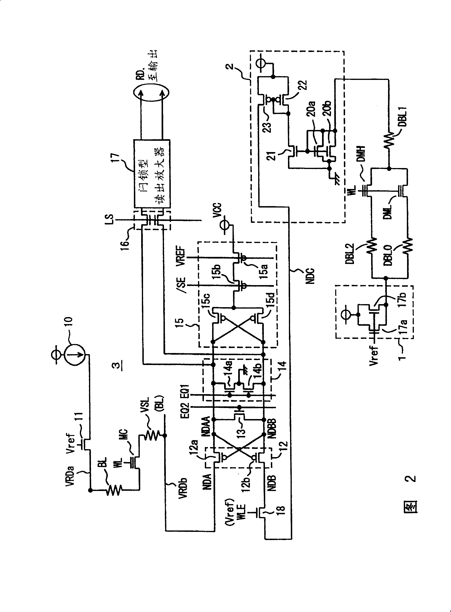
[0175] FIG. 5 is a diagram schematically showing the configuration of important parts of a nonvolatile semiconductor memory according to Embodiment 2 of the present invention. The structure shown in FIG. 5 differs from the structure shown in FIG. 1 in the following points. That is, when data is read, a dummy read current i is supplied to dummy bit lines DBL0 and DBL2 , and a reference current generating circuit 30 that generates the average current and sends it to the current amplifier circuit 3 is provided. In addition, dummy bit line DBL1 is connected to the ground node through this read selection gate TT1 when data is read. The other structures are the same as those shown in FIG. 1, and the corresponding parts are denoted by the same reference numerals, and detailed description thereof will be omitted.

[0176] In the configuration shown in FIG. 5, dummy bit line DBL1 is connected to the ground node when data is read. The reference current generating circuit 30 supplies a...

Embodiment 3

[0187] FIG. 7 is a structural diagram showing important parts of a nonvolatile semiconductor memory according to Embodiment 3 of the present invention. In FIG. 7, the current sense / amplifier circuit 3 has the same structure as that of the first and second embodiments. However, this current read / amplifier circuit 3 compares the current flowing through the internal read data line VRDa with the current supplied from the subtraction circuit 45 , unlike the first and second embodiments described above. That is, in the configuration shown in FIG. 7 , the current sense / amplifier circuit 3 uses the current obtained by subtracting the current flowing through the memory cell from the reference current as a comparison object.

[0188] In this third embodiment, dummy cells DM and normal cells MC are arranged in a straight line within the same array. The structure of the memory cell array in Embodiment 3 is the same as that of the memory cell array shown in FIG. 1 or FIG. 5 .

[0189] In...


PUM


Abstract

Dummy cells in an erased state and in a write state are used to generate a dummy current corresponding to the average current of currents flowing in the dummy cells using a 1 / 2 current generating circuit, and the dummy current is compared with a current corresponding to a memory cell current flowing in a selected normal cell using a current sense amplification circuit to generate internal read data according to a result of the comparison. With such a configuration, a non-volatile semiconductor memory device capable of reading data at high speed can be achieved.

Description

technical field [0001] The present invention relates to a nonvolatile semiconductor memory, and more particularly to a structure for high-speed readout of data in a nonvolatile semiconductor memory. More specifically, the present invention relates to a data readout structure for a nonvolatile semiconductor memory having an insulating film charge trap type memory cell that stores charges in an insulating film. Background technique [0002] As a memory that stores information in a non-volatile manner, a bulk-erasable EEPROM (read-only memory that can be electrically written / erased) has memory cells formed of stacked gate field effect transistors. In this bulk-erase EEPROM, charges are stored in a floating gate insulated from its surroundings, for example, made of polysilicon, and the threshold voltage of a memory cell transistor is changed according to the amount of stored charges to store information. [0003] In the case of a nonvolatile memory cell structure using this sta...

Claims


Application Information

Patent Timeline
Patent Type & Authority Patents(China)
IPC IPC(8): G11C16/06H01L29/792G11C11/56G11C16/04G11C16/28H01L21/8247H01L27/10H01L27/115H01L29/788
CPCG11C11/5671G11C16/0475G11C16/28
Inventor 大石司
Owner MITSUBISHI ELECTRIC CORP
Why Eureka
Try Eureka