Electron beam photoetching method for fabricating T-shaped grid structure

A technology of electron beam lithography and grid structure, which is applied in the field of microwave communication, can solve problems such as process failure, achieve the effects of avoiding incompatibility of developer, convenient and reliable preparation, and avoiding peeling failure

Active Publication Date: 2018-03-30
XIDIAN UNIV
View PDF7 Cites 18 Cited by
  • Summary
  • Abstract
  • Description
  • Claims
  • Application Information

AI Technical Summary

Problems solved by technology

see image 3 (a), metal is deposited after single-layer photolithography development, but because the sidewall of the photoresist is easy to adhere to some metals, when the metal on the photoresist is peeled off (using a chemical solution to dissolve the photoresist), there will be materials The effective metal on the surface is peeled off together, causing the process to fail

Method used


Image

  • Electron beam photoetching method for fabricating T-shaped grid structure
  • Electron beam photoetching method for fabricating T-shaped grid structure
  • Electron beam photoetching method for fabricating T-shaped grid structure

Examples


Embodiment Construction

[0032] The present invention will be described in further detail below in conjunction with the accompanying drawings.

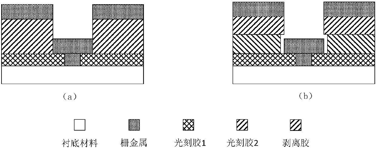
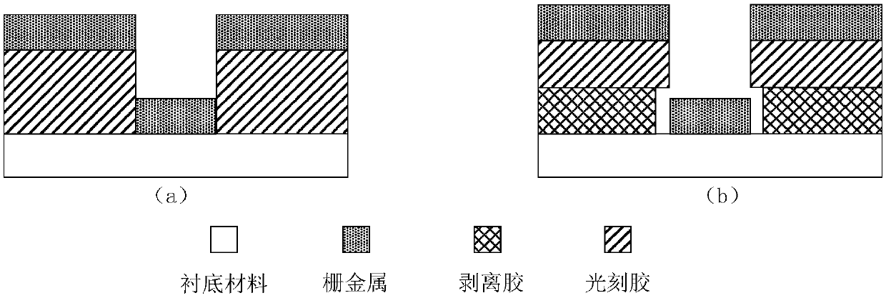
[0033] see Figure 4 , the present invention makes the electron beam lithography method of T-shaped grid structure and comprises the following steps:

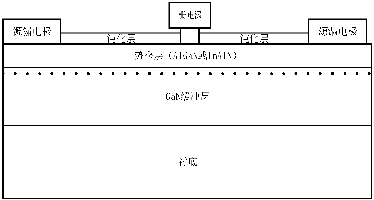
[0034] 1. On the substrate material, coat No. 1 photoresist and bake at 180°C for 2 minutes. The photoresist uses PMMA glue, which has the characteristics of low sensitivity and high photoresist dose; the substrate material adopts GaN-based heterojunction planar materials;

[0035] 2. Coating No. 2 photoresist, the photoresist is PMMA-MAA glue, and baked at 200°C for 5 minutes. The sensitivity of PMMA-MAA glue is higher than that of PMAA glue, and the photoresist dose is lower than that of PMMA glue;

[0036] 3. Coating No. 3 photoresist, this photoresist still adopts PMMA-MAA glue and bakes, and this baking temperature will be lower than No. 2 photoresist above 20 ℃, in the embodiment, bake 5 at 160 ℃ minu...


PUM


Abstract

An electron beam photoetching method for fabricating a T-shaped grid structure comprises the following steps of coating first photoresist with low sensitivity and high photoetching dosage on a GaN heterojunction planar material, and performing baking; coating second photoresist on the first photoresist, and performing baking, wherein the second photoresist employs PMMA-MMA glue, the sensitivity ofthe PMMA-MMA glue is higher than that of PMAA, and the photoetching dosage is lower than that of PMMA; coating third photoresist on the second photoresist, and performing baking, wherein the third photoresist still employs PMMA-MMA glue, and a baking temperature of the third photoresist is lower than a baking temperature of the second photoresist; and finally forming the T-shaped grid structure with an undercut structure by electron beam photoetching, developing and stripping processes. By the electron beam photoetching method, a T-shaped grid can be more convenient and reliable to fabricate.

Description

technical field [0001] The invention relates to the field of microwave communication, in particular to an electron beam photolithography method for manufacturing a T-shaped grid structure. Background technique [0002] With the continuous development of wireless networks, mobile phone communications, television broadcasting, and aerospace systems, the application of microwave communications has covered almost all human activities and has increasingly become an indispensable part of life. [0003] The core of the microwave communication system is the microwave power amplifier, which is also the most expensive component in the system. It plays the role of signal amplification and high-power output. Its performance directly determines the working effect of the microwave communication system. The core of the microwave power amplifier is the microwave power device. Although Si-based devices have mature technology, high reliability and low cost, due to the dual limitations of thei...

Claims


Application Information

Patent Timeline
Patent Type & Authority Applications(China)
IPC IPC(8): H01L21/027H01L21/28
CPCH01L21/0272H01L21/0277H01L29/401
Inventor 张鹏杨眉马晓华郝跃武盛
Owner XIDIAN UNIV
Why Eureka
Try Eureka