Organic light-emitting diode (OLED) display device and fabrication method thereof

A display device and electrode technology, which is applied in the manufacture of semiconductor/solid-state devices, electrical components, and electrical solid-state devices, etc., can solve the problems of organic layer damage, easy to cause microcavity effect, and unfavorable device performance.

Inactive Publication Date: 2018-03-30
WUHAN CHINA STAR OPTOELECTRONICS TECH CO LTD
View PDF4 Cites 2 Cited by
  • Summary
  • Abstract
  • Description
  • Claims
  • Application Information

AI Technical Summary

Problems solved by technology

Top-emission OLED display devices generally use a reflective metal bottom electrode and a transparent or translucent top electrode. Among them, the transparent electrode is generally a conductive metal oxide, but its high-energy manufacturing process will cause damage to the organic layer, which is not conducive to maintaining device performance; The transparent top electrode generally adopts a thin metal layer. In order to maintain its conductivity, the thin metal layer generally has a thickness of 10-15nm. The metal film

Method used


Image

  • Organic light-emitting diode (OLED) display device and fabrication method thereof
  • Organic light-emitting diode (OLED) display device and fabrication method thereof
  • Organic light-emitting diode (OLED) display device and fabrication method thereof

Examples


Embodiment Construction

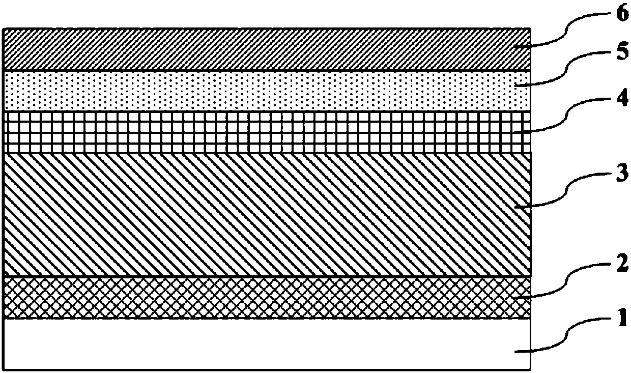
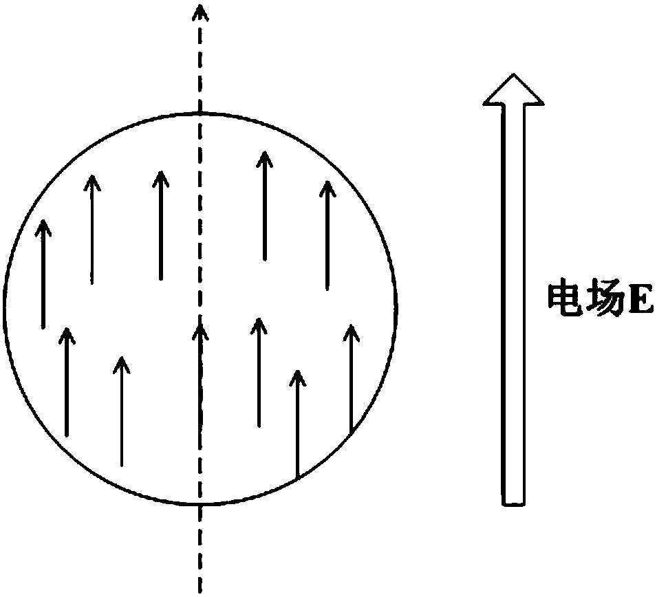
[0040] The present invention provides an OLED display device, such as figure 1 As shown, the OLED display device includes a base substrate 1, a first electrode 2, an organic functional layer 3, a second electrode 4, a polymer dispersed liquid crystal layer 5, and an upper electrode 6 stacked in sequence, wherein the first electrode 2 is opaque electrode, the second electrode 4 is a translucent electrode. Wherein, the first electrode 2, the organic functional layer 3 and the second electrode 4 form a microcavity structure, forming a microcavity effect; when the OLED display device is working, the absolute value of the voltage difference between the first electrode 2 and the second electrode 4 is 0 (that is, the electric field strength between the first electrode 2 and the second electrode 4 is 0) or greater than 0. The OLED display device is a top emission type OLED display device.

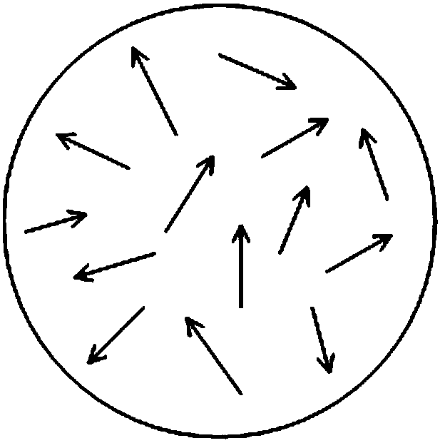
[0041] Polymer Dispersed Liquid Crystal (PDLC, Ploymer Dispersed Liquid Crystal) is one of th...


PUM


Abstract

The invention provides an organic light-emitting diode (OLED) display device and a fabrication method thereof. The OLED display device comprises a substrate, a first electrode, an organic functional layer, a second electrode, a polymer dispersion liquid crystal layer and an upper part which are sequentially laminated, wherein the first electrode is a non-transparent electrode, the second electrodeis a semi-transparent electrode, and the first electrode, the organic functional layer and the second electrode form a microcavity structure. By the OLED display device, damage to the organic functional layer is prevented, the peeping prevention function can be achieved, the privacy of display content of the OLED display device is ensured, and the display content of the OLED display device also can be viewed clearly from each angle.

Description

technical field [0001] The invention relates to the field of display technology, in particular to an OLED display device and a preparation method thereof. Background technique [0002] Organic Light-Emitting Diode (OLED) has the advantages of self-illumination, fast response, wide viewing angle, high brightness, thin and flexible, etc., its potential market prospect is optimistic by the industry, and it has become the next generation of display technology. The main direction of development. [0003] According to different light extraction methods, OLED display devices can be divided into bottom emission type and top emission type. The light of the top emission type OLED display device is extracted from the top. This device structure can greatly increase the aperture ratio of the display panel. Top-emission OLED display devices generally use a reflective metal bottom electrode and a transparent or translucent top electrode. Among them, the transparent electrode is generally ...

Claims


Application Information

Patent Timeline
IPC IPC(8): H01L51/52H01L51/56H01L27/32
CPCH10K59/12H10K50/805H10K50/85H10K50/86H10K71/00
Inventor 邢磊
Owner WUHAN CHINA STAR OPTOELECTRONICS TECH CO LTD
Why Eureka
Try Eureka