

Mask, memory and manufacturing method of memory
A manufacturing method and mask technology, which is applied in the field of memory and memory manufacturing and mask, can solve the problems of difficult registration of mask and lower memory quality, etc., so as to improve registration accuracy, improve quality and reliability Effect
- Summary
- Abstract
- Description
- Claims
- Application Information
AI Technical Summary
Problems solved by technology
Method used
Image

Examples
Embodiment Construction
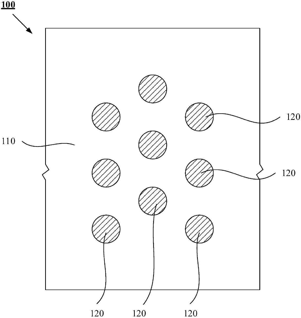
[0104] First, please refer to figure 1 , which is a structural schematic diagram of a mask for forming a storage node contact in a memory. Such as figure 1 As shown, the mask plate 100 includes: a substrate 110 having a plurality of storage node contact patterns 120 , and the storage node contact patterns 120 are circular.
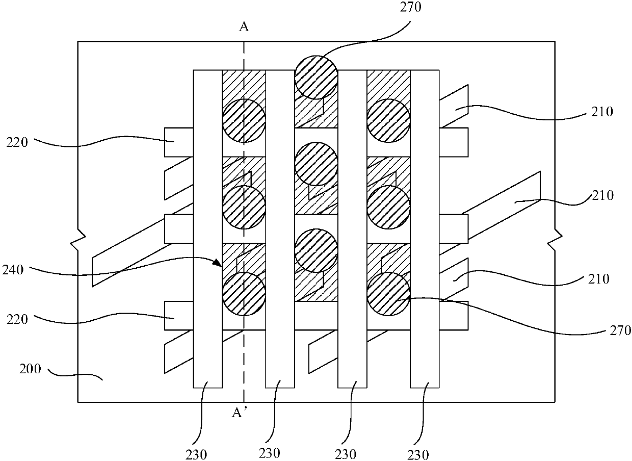
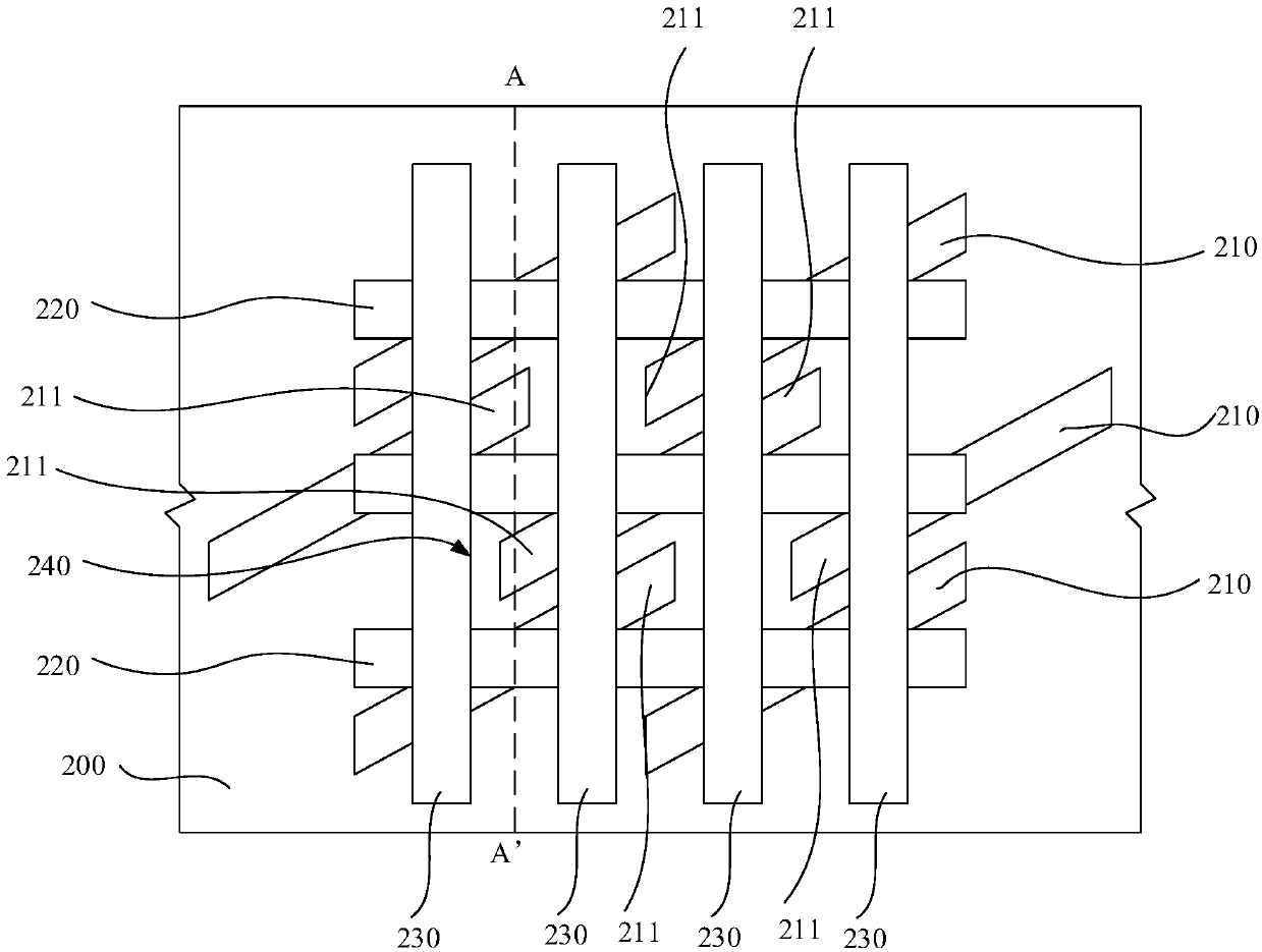
[0105] Next, please refer to Figure 2 to Figure 8 ,in, figure 2 is adopted figure 1 The schematic top view of the memory after the mask plate forms the contact with the storage node as shown; image 3 yes figure 2 A schematic top view of the substrate in the shown memory; Figure 4 yes figure 2 A schematic cross-sectional view of the substrate along AA' in the shown memory; Figure 5 is in Figure 4 Schematic diagram of the structure after the connection material layer is formed on the shown structure; Figure 6 is in Figure 5 Schematic diagram of the structure after forming the first photoresist layer on the shown structure; Figure 7 is ...
PUM
 Abstract
Description
Claims
Application Information