Driving system of GaN power device
A technology for driving systems and power devices, applied in the application field of GaN power devices, can solve the problems of false turn-on of oscillation peaks, high power loss of GaN driving circuits, low gate threshold voltage, etc. Loss problem, effect of slowing ascent
- Summary
- Abstract
- Description
- Claims
- Application Information
AI Technical Summary
Problems solved by technology
Method used
Image
Examples
Embodiment Construction
[0022] Now, the present invention will be further explained and described by combining specific embodiments and accompanying drawings.
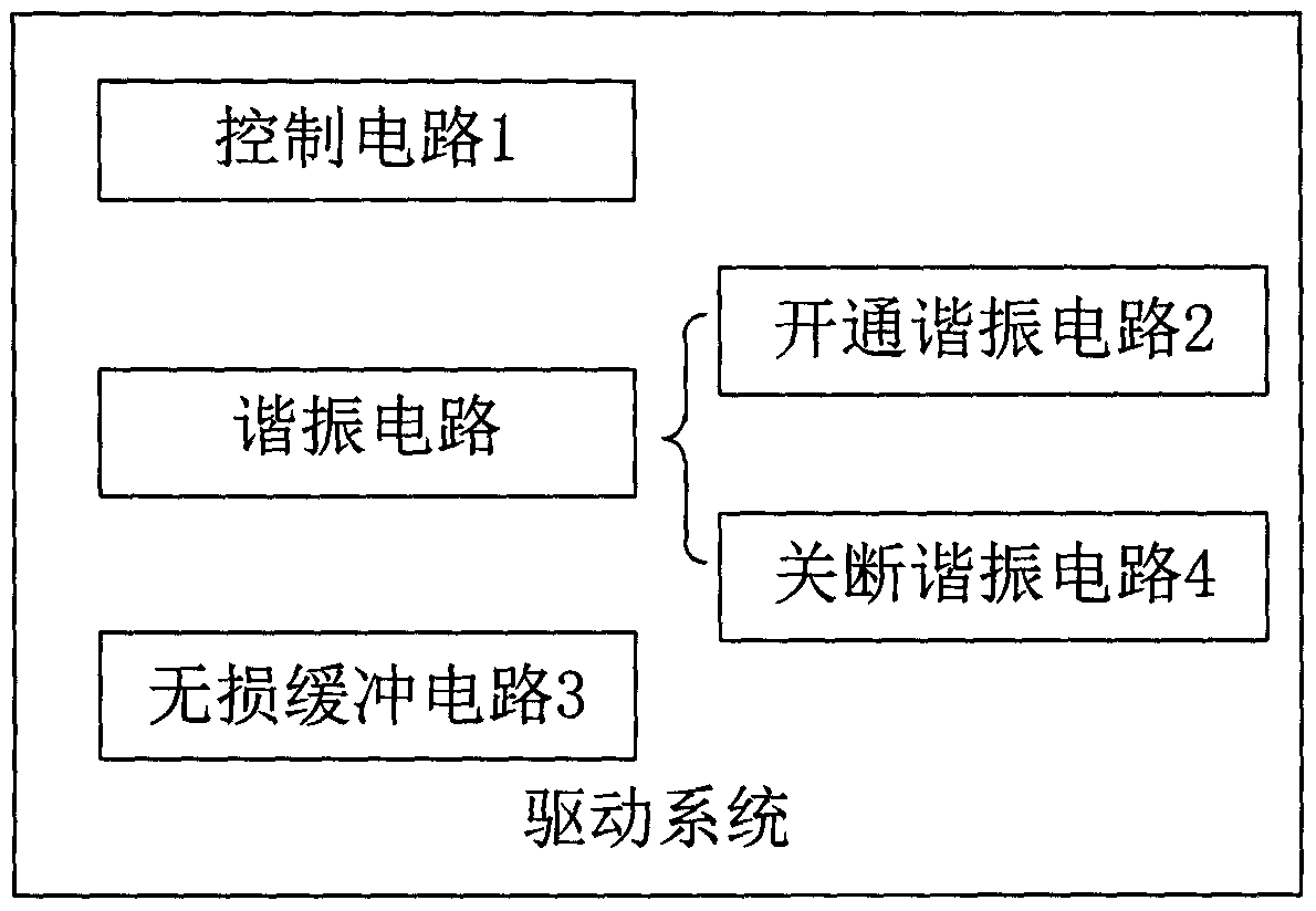
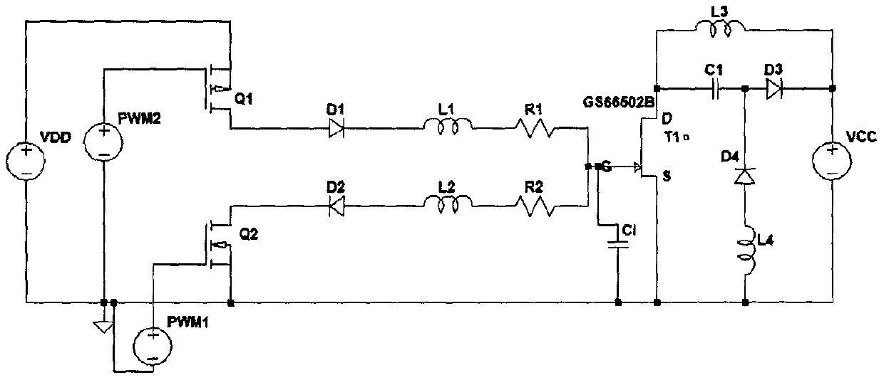
[0023] figure 1 It is the overall structural block diagram of the drive system. from figure 1 It can be seen from the figure that the drive system applicable to GaN power devices in the present invention includes a control circuit 1, a turn-on resonant circuit 2, a turn-off resonant circuit 4 and a lossless buffer circuit 3. The control circuit is used to generate two PWM signals to drive the auxiliary switch tube conduction; the resonant circuit is used to realize the turn-on and turn-off of GaN T1; the lossless snubber circuit is used to slow down the rising speed of the drain voltage of the main switch tube T1, and protect the main switch tube T1.
[0024] In the above embodiment, the control circuit includes upper and lower PWM outputs, which can control the gate driving voltage of the auxiliary switching tube, and the gate driving volt...
PUM
 Abstract
Description
Claims
Application Information


