Fin-type field-effect tube and forming method therefor

A technology of fin field effect transistors and fins, which is applied in the direction of transistors, electrical components, electric solid devices, etc., can solve the problems that the electrical performance of fin field effect transistors needs to be improved, achieve good lattice integrity, and improve electrical performance , the effect of good electrical properties

Active Publication Date: 2018-04-17
SEMICON MFG INT (SHANGHAI) CORP +1
View PDF8 Cites 4 Cited by
  • Summary
  • Abstract
  • Description
  • Claims
  • Application Information

AI Technical Summary

Problems solved by technology

[0004] However, the electrical performance of the fin field effect transistor formed by the prior art needs to be improved

Method used


Image

  • Fin-type field-effect tube and forming method therefor
  • Fin-type field-effect tube and forming method therefor
  • Fin-type field-effect tube and forming method therefor

Examples


Embodiment Construction

[0013] It can be seen from the background art that the electrical performance of the fin field effect transistor formed in the prior art needs to be improved. This problem is more significant for N-type fin field effect transistors. Analyze the reasons for this:

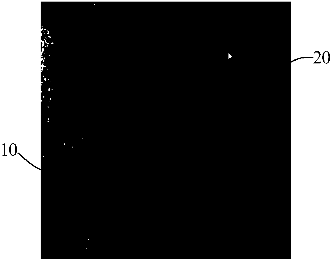
[0014] combined reference figure 1 , showing an electron microscope image of a fin field effect transistor. For an N-type fin field effect transistor, the current main formation method includes forming recesses in the fins 10 on both sides of the gate structure (not shown). A groove (not shown in the figure); an in-situ doped epitaxial layer 20 is formed in the groove by a selective epitaxy process, and the in-situ doped epitaxial layer 20 has N-type dopant ions.

[0015] However, since the surface of the fin portion 10 exposed by the groove has a crystal orientation, during the selective epitaxy process, the in-situ doped epitaxial layer 20 grows along the crystal orientation; and The crystal orientation is di...


PUM


Abstract

The invention discloses a fin-type field-effect tube and a forming method therefor. The method comprises the steps: providing a substrate with a plurality of split fin parts, wherein the substrate comprises an NMOS region; forming a pseudo-gate structure which stretches across the fin parts and covers the top surfaces and side wall surfaces of a part of fin parts, and comprises a gate oxidation layer and a pseudo-gate electrode layer located on the gate oxidation layer; carrying out the etching of a part of fin parts at two sides of the pseudo-gate structure in the NMOS region by certain thickness, forming NMOS region grooves in the fin parts of the NMOS region, wherein the profile of each NMOS region groove in a direction perpendicular to the extending direction of the fin parts is shapedlike U; and forming an in-situ doped epitaxial layer with N-type doped atoms in the NMOS region grooves. According to the invention, the NMOS region grooves are formed in the fin parts at two sides of the pseudo-gate structure in the NMOS region, and the profile of each NMOS region groove in the direction perpendicular to the extending direction of the fin parts is shaped like U. The surfaces ofthe fin parts exposed by the NMOS region grooves are in <100> crystal orientation, and the in-situ doped epitaxial layer grows in the <100> crystal orientation, so the dislocation of the in-situ dopedepitaxial layer is smaller.

Description

technical field [0001] The invention relates to the field of semiconductors, in particular to a fin field effect transistor and a forming method thereof. Background technique [0002] In semiconductor manufacturing, with the development trend of VLSI, the feature size of integrated circuits continues to decrease. In order to accommodate the reduction in feature size, the channel length of MOSFETs has also been shortened accordingly. However, as the channel length of the device is shortened, the distance between the source and the drain of the device is also shortened, so the control ability of the gate to the channel becomes worse, and the gate voltage pinches off the channel. The difficulty is also increasing, making the phenomenon of subthreshold leakage (subthreshold leakage), the so-called short-channel effect (SCE: short-channel effects) more likely to occur. [0003] Therefore, in order to better adapt to the reduction of the feature size, the semiconductor process g...

Claims


Application Information

Patent Timeline
Patent Type & Authority Applications(China)
IPC IPC(8): H01L21/8238H01L27/092H01L29/06
CPCH01L21/823821H01L27/0924H01L29/0684
Inventor 李勇
Owner SEMICON MFG INT (SHANGHAI) CORP
Why Eureka
Try Eureka