Optical imaging system

A technology of optical imaging system and imaging surface, applied in optics, optical components, TV system components, etc., can solve problems such as inability to meet photography requirements, achieve optimal optical path adjustment ability, improve imaging quality, and reduce sensitivity

Active Publication Date: 2018-04-27
ABILITY OPTO ELECTRONICS TECH
View PDF4 Cites 32 Cited by
  • Summary
  • Abstract
  • Description
  • Claims
  • Application Information

AI Technical Summary

Problems solved by technology

[0003] The traditional optical system mounted on portable devices mostly adopts a two-piece lens structure. However, due to the continuous improvement of pixels in portable devices and the demand for large apertures by end consumers, such as low-light and night shooting functions, the existing optical imaging The system can no longer meet the higher-level photography requirements

Method used


Image

  • Optical imaging system
  • Optical imaging system
  • Optical imaging system

Examples


no. 1 example

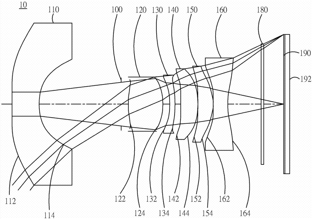
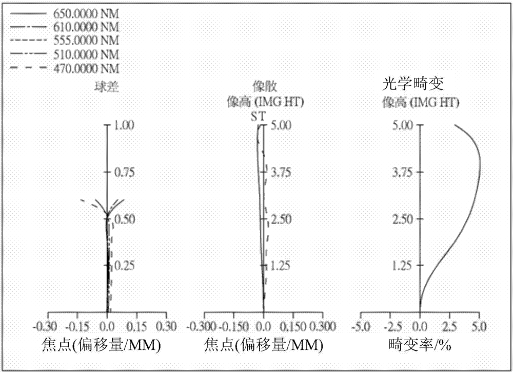
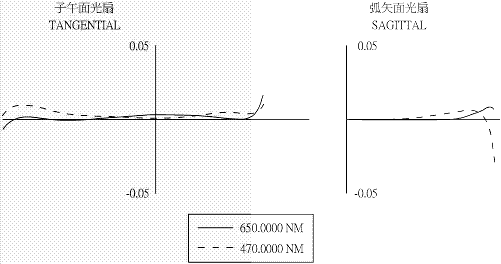
[0220] Please refer to Figure 1A and Figure 1B ,in Figure 1A It shows a schematic diagram of an optical imaging system according to the first embodiment of the present invention, which is composed of six lenses with refractive power and can provide good imaging for visible light and infrared light at the same time, Figure 1B From left to right are the spherical aberration, astigmatism and optical distortion curves of the optical imaging system of the first embodiment. Figure 1C It is the lateral aberration diagram of the meridian plane light fan and the sagittal plane light fan of the optical imaging system of the first embodiment, the longest working wavelength and the shortest working wavelength passing through the edge of the aperture at the 0.7 field of view. Figure 1D It shows the through focus modulation conversion ratio transfer rate diagram (Through Focus MTF) of the central field of view, 0.3 field of view, and 0.7 field of view of the visible light spectrum of ...

no. 2 example

[0292] Please refer to Figure 2A and Figure 2B ,in Figure 2A It shows a schematic diagram of an optical imaging system according to the second embodiment of the present invention, which is composed of seven lenses with refractive power and can provide good imaging for visible light and infrared light at the same time, Figure 2B From left to right are the spherical aberration, astigmatism and optical distortion curves of the optical imaging system of the second embodiment. Figure 2C It is a lateral aberration diagram of the optical imaging system of the second embodiment at a field of view of 0.7. Figure 2D It shows the defocus modulation conversion versus transfer ratio diagram of the central field of view, 0.3 field of view, and 0.7 field of view of the visible light spectrum in this embodiment; Figure 2E It shows the through-focus modulation conversion versus transfer ratio diagrams of the central field of view, 0.3 field of view, and 0.7 field of view of the infra...

no. 3 example

[0317] Please refer to Figure 3A and Figure 3B ,in Figure 3A It shows a schematic diagram of an optical imaging system according to the third embodiment of the present invention, which is composed of six lenses with refractive power and can provide good imaging for visible light and infrared light at the same time, Figure 3B From left to right are the spherical aberration, astigmatism and optical distortion curves of the optical imaging system of the third embodiment. Figure 3C It is a lateral aberration diagram of the optical imaging system of the third embodiment at a field of view of 0.7. Figure 3D The defocus modulation conversion versus transfer rate diagrams of the central field of view, 0.3 field of view, and 0.7 field of view of the visible light spectrum of this embodiment are shown; Figure 3E shows the central field of view, 0.3 field of view of the infrared light spectrum of this embodiment. Through-focus modulation conversion vs. transfer rate plots for FO...


PUM

PropertyMeasurementUnit
wavelengthaaaaaaaaaa

Abstract

The invention discloses an optical imaging system. The optical imaging system comprises an imaging lens group and an image sensor. The imaging lens group comprises at least three lenses with refraction power, a first imaging surface and a second imaging surface. The image sensor is arranged between the first imaging surface and the second imaging surface. The first imaging surface is a visible light image plane specifically vertical to an optical axis. Additionally, the center visual field of the first imaging surface has the maximum value of modulation transfer factor with first space frequency. The second imaging surface is an infrared light image plane specifically vertical to the optical axis. Additionally, the center visual field of the second imaging surface has the maximum value ofmodulation transfer factor with first space frequency. When a specific condition is met, the distance relative to the imaging focal length of visible light and the distance relative to the imaging focal length of infrared light are reduced. Meanwhile, imaging quality of visible light and infrared light is enhanced.

Description

technical field [0001] The invention relates to an optical imaging system, and in particular to a miniaturized optical imaging system applied to electronic products. Background technique [0002] In recent years, with the rise of portable electronic products with photography functions, the demand for optical systems has increased day by day. The photosensitive component of the general optical system is nothing more than two types of photosensitive coupling device (Charge Coupled Device; CCD) or complementary metal-oxide semiconductor sensor (Complementary Metal-Oxide Semiconductor Sensor; CMOSSensor), and with the advancement of semiconductor technology, making The pixel size of photosensitive components is shrinking, and the optical system is gradually developing into the high-pixel field, so the requirements for image quality are also increasing. [0003] The traditional optical system mounted on portable devices mostly adopts a two-piece lens structure. However, due to t...

Claims


Application Information

Patent Timeline
Patent Type & Authority Applications(China)
IPC IPC(8): G02B13/14G02B13/00H04N5/225
CPCG02B13/004G02B13/0045G02B13/14H04N23/55G02B1/04G02B9/62G02B9/64G02B13/008G02B13/0055
Inventor 张永明赖建勋廖国裕刘耀维
Owner ABILITY OPTO ELECTRONICS TECH
Why Eureka
Try Eureka