High-speed programming device supporting various communication modes

A communication method and burner technology, which is applied in software deployment and other directions, can solve problems such as the inability to meet the programming and upgrading of the main control chip and peripheral storage devices, the low transmission rate of the CAN bus, and the difficulty of testing and upgrading, etc., to achieve convenient Upgrading and maintenance, ingenious overall structure design, convenient disassembly, assembly, maintenance and replacement

Pending Publication Date: 2018-05-01
YANFENG VISTEON ELECTRONICS TECH NANJING
View PDF0 Cites 9 Cited by
  • Summary
  • Abstract
  • Description
  • Claims
  • Application Information

AI Technical Summary

Problems solved by technology

[0003] (1) Offline programming: memory chips are programmed before SMT placement, but later testing and upgrading will be difficult to achieve
[0004] (2) Semi-offline programming: After the memory chip is placed on the SMT, the SPI (Serial Peripheral Interface, Serial Peripheral Interface) data line and power line are drawn out for programming, but this kind of later upgrade without disassembly is also difficult to achieve , and connecting to the power supply is easy to cause the MCU (Micro controller unit) of the car combination instrument control motherboard to self-lock and start abnormally
[0005] (3) CAN bus burning: burn the memory chip through the CAN bus, but the transmission rate of the CAN bus is relatively low, resulting in a long burning time
[0006] Therefore, the programming method adopted by the burner in the prior art has been unable to meet the programming and upgrading of the main control chip and peripheral storage devices on the control board of the automobile instrument cluster, and a new type of burner is urgently needed to solve the problem. Problems in the above three burning methods

Method used


Image

  • High-speed programming device supporting various communication modes
  • High-speed programming device supporting various communication modes
  • High-speed programming device supporting various communication modes

Examples


Embodiment Construction

[0025] In order to deepen the understanding and recognition of the present invention, the present invention will be further described and introduced below in conjunction with the accompanying drawings.

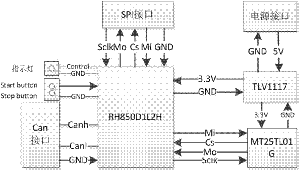
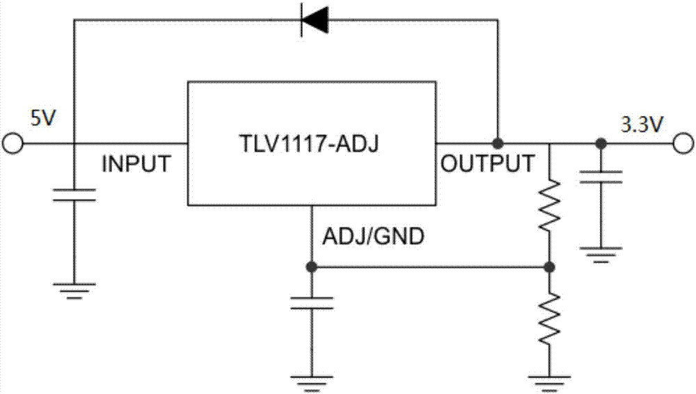
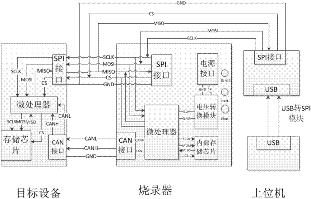
[0026] Such as figure 1 As shown, a high-speed programmer supporting multiple communication methods is given, including a PCB board, which is equipped with a microprocessor RH850D1L, an internal memory chip MT25TL01G, a voltage conversion module, a power interface, an SPI interface, CAN interface, external signal trigger button, the microprocessor has 2 groups of SPI signal lines, the internal storage chip MT25TL01G is connected to the microprocessor through a group of SPI signal lines, and the SPI interface is connected to the microprocessor through another group of SPI signal lines Microprocessor connected. Wherein, a group of SPI signal lines arranged between the microprocessor and the internal memory chip include SCLK ports, MOSI ports, MISO ports, and CS ports, and a gro...


PUM


Abstract

The invention relates to a high-speed programming device supporting various communication modes. The programming device includes a PCB (Printed Circuit Board) board. A microprocessor, an internal storage chip, a voltage conversion module, a power supply interface, an SPI (Serial Peripheral Interface) interface, a CAN interface and external signal triggering buttons are arranged on the PCB board. The microprocessor has 2 or more sets of SPI signal lines. The internal storage chip is connected with the microprocessor through a set of the SPI signal lines. The SPI interface is connected with themicroprocessor through the remaining SPI signal lines. Output ends of the voltage conversion module are connected with power supply ends and ground ends of the microprocessor and the internal storagechip. The CAN interface is connected with CAN H/L ports of the microprocessor. The external signal triggering buttons are connected with I/O ports of the microprocessor. The power supply interface isconnected with input ends of the voltage conversion module. The high-speed programming device is portable, is easy to carry and operate, and is suitable for use in offline upgrading of ECUs (electronic control units) of automobile combined-instruments and the like and online upgrading after automobile installation.

Description

technical field [0001] The invention belongs to the technical field of automotive electronics, and in particular relates to a peripheral storage device and a main control chip programming used in an automotive electronic circuit, in particular to a main controller used in a vehicle ECU (electronic control unit) It is a high-speed programmer for burning peripheral memory chips, which supports burning methods of various communication protocols. Background technique [0002] With the continuous development of the automobile industry, the functions of the automobile instrument cluster are becoming more and more abundant, and the number of later upgrades and inspections tends to increase. At present, the programming method of the main control chip and peripheral storage devices on the control board of the automobile instrument cluster There are mainly three types: [0003] (1) Offline programming: The memory chip is programmed before SMT placement, but it will be difficult to ac...

Claims


Application Information

Patent Timeline
Patent Type & Authority Applications(China)
IPC IPC(8): G06F8/61
CPCG06F8/61
Inventor 刘昌元王仁杰黄雷陈元珩朱瑞杰杨浩修
Owner YANFENG VISTEON ELECTRONICS TECH NANJING
Why Eureka
Try Eureka