Manufacturing method of printed circuit board realizing any layer interconnection

A printed circuit board and any layer interconnection technology, applied in the field of circuit board manufacturing, to achieve the effect of suitable promotion and simple processing technology

Inactive Publication Date: 2018-05-04
赣州市深联电路有限公司
View PDF7 Cites 12 Cited by
  • Summary
  • Abstract
  • Description
  • Claims
  • Application Information

AI Technical Summary

Problems solved by technology

However, this technology is mainly reflected in the lamination technology of multi-layer boards, which is only suitable for lamination of ten-layer boards and three-stage HDI circuit boards.

Method used


Image

  • Manufacturing method of printed circuit board realizing any layer interconnection
  • Manufacturing method of printed circuit board realizing any layer interconnection
  • Manufacturing method of printed circuit board realizing any layer interconnection

Examples


Embodiment Construction

[0027] In order to make the object, technical solution and advantages of the present invention clearer, the present invention will be further described in detail below in conjunction with the accompanying drawings and embodiments. It should be understood that the specific embodiments described here are only used to explain the present invention, not to limit the present invention.

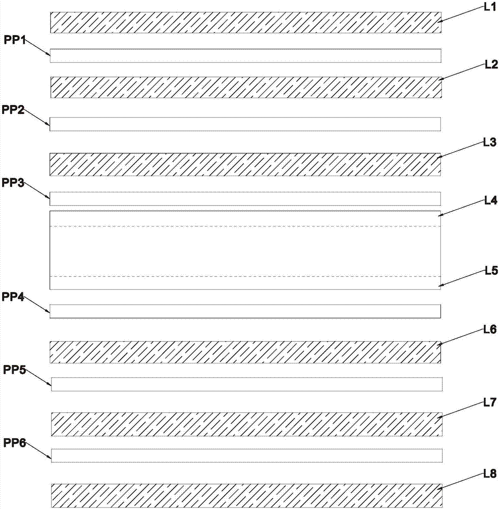
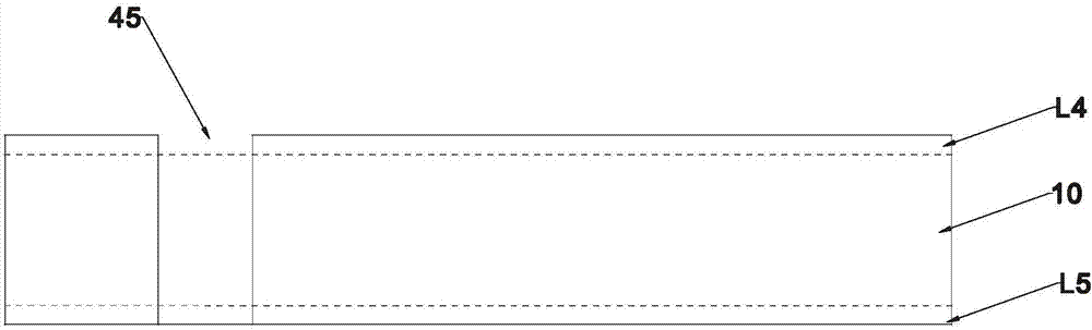
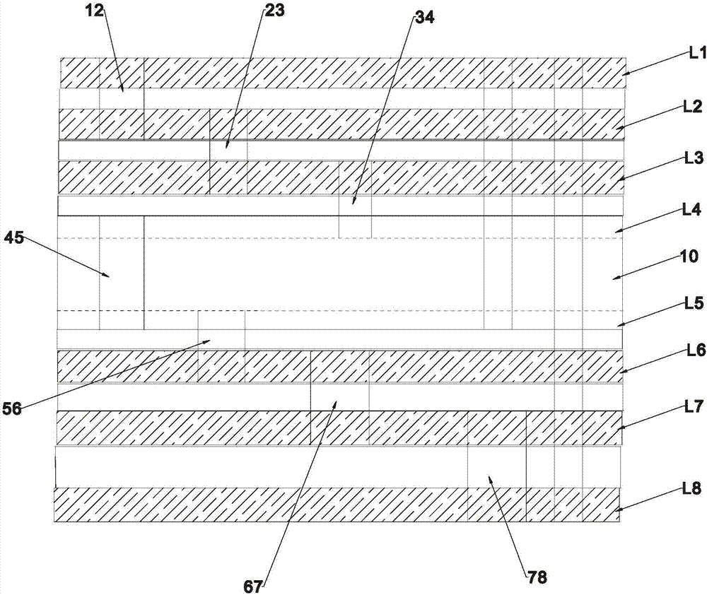
[0028] The invention provides a method for manufacturing a printed circuit board with any layer interconnection. In the method, blind holes are drilled from the upper surface of the inner core board to the lower surface, and one of the blind holes is made to pass through the copper foil layer and the upper surface of the core board. The dielectric insulation layer of the inner core board reaches the copper foil layer on the lower surface of the core board; then the above-mentioned blind holes are subjected to hole metallization treatment and electroplating and hole filling treatment, and the filled ...


PUM


Abstract

The invention provides a manufacturing method of a printed circuit board realizing any layer interconnection. According to the method, after a hole is drilled in an inner core board, electroplating filling is performed, blind holes are drilled after outer boards are pressed on the inner core board, and electroplating filling is performed on the blind holes. Interconnection of inner and outer boards is realized through electroplating filling of the blind holes. Compared with the prior art, the method realizes four-level HDI any layer interconnection and hole stacking of eight-layer printed circuit board and has the advantages that the processing technology is simple, the method is suitable for popularization and the like.

Description

technical field [0001] The present invention relates to the technical field of circuit board manufacturing, in particular to a method for manufacturing an arbitrary-layer interconnection printed circuit board, in particular to a method for realizing 4-level HDI arbitrary-layer interconnection and stacked holes on an 8-layer printed circuit board method. Background technique [0002] With the rapid development of miniaturization and high integration of electronic products, higher requirements are put forward for the thinner and higher density of printed circuit boards of electronic product carriers. For printed circuit boards, any-layer interconnection is the highest-order high-density interconnection (HDI) process. Compared with traditional printed circuit boards, the size of any-layer interconnection is relatively reduced by 50%, but it can increase the number of layers by 30%. Interconnection capability is a new trend in the development of printed circuit boards. At pres...

Claims


Application Information

Patent Timeline
Patent Type & Authority Applications(China)
IPC IPC(8): H05K3/42H05K3/46
CPCH05K3/429H05K3/4644H05K2203/0214
Inventor 曹宝龙文泽生王泉勇
Owner 赣州市深联电路有限公司
Why Eureka
Try Eureka