MEMS stereoscopic packaging-assembling oriented solder ball bump bonding method

A three-dimensional packaging and bonding technology, which is applied to the photoengraving process of the pattern surface, the microstructure device, the processing microstructure device, etc. The packaging bonding process has not achieved standardization and other issues, achieving the effects of high-efficiency and high-precision MEMS device packaging, high degree of automation, and wide adaptability

Inactive Publication Date: 2010-10-13
HARBIN INST OF TECH
View PDF5 Cites 11 Cited by
  • Summary
  • Abstract
  • Description
  • Claims
  • Application Information

AI Technical Summary

Problems solved by technology

[0005] The purpose of the present invention is to solve the problem that the packaging and bonding process of the existing MEMS devices has not been standardized. The automatic bonding technology of the existing MEMS devices is only applicable to the laser bump production of a specific pad plane, and cannot integrate the bump production and interconnection. It is not suitable for three-dimensional packaging of MEMS devices, and a solder ball bump bonding method for three-dimensional packaging and assembly of MEMS is provided.

Method used


Image

  • MEMS stereoscopic packaging-assembling oriented solder ball bump bonding method
  • MEMS stereoscopic packaging-assembling oriented solder ball bump bonding method
  • MEMS stereoscopic packaging-assembling oriented solder ball bump bonding method

Examples


specific Embodiment approach 1

[0038] Specific implementation mode 1: the following combination figure 1 , figure 2 with Figure 4 To illustrate this embodiment, this embodiment is completed based on the following equipment: chip clamping mechanism 1, image acquisition device 2, suction nozzle 3, laser head 4, laser to fiber coupler 5, optical fiber 6, and laser self-focusing lens 7, laser self-focusing lens The focusing lens 7 and the suction nozzle 3 are coaxially clamped,

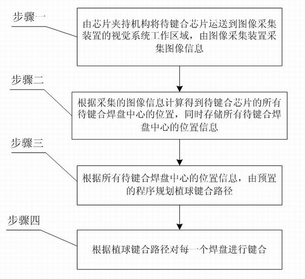
[0039] Its bonding method includes the following steps:

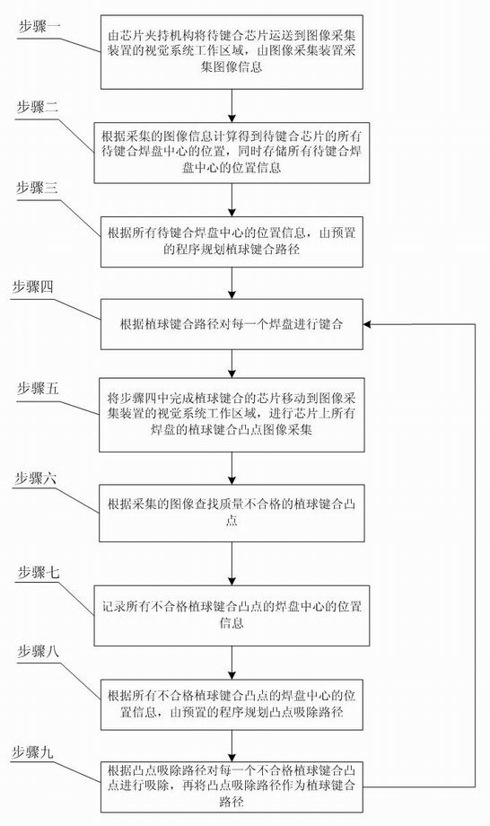
[0040] Step 1: The chip to be bonded is transported to the working area of ​​the vision system of the image acquisition device 2 by the chip clamping mechanism 1, and the image information is collected by the image acquisition device 2;

[0041] Step 2: Calculate the positions of the centers of all the bonding pads of the chip to be bonded according to the collected image information, and store the position information of the centers of all the bonding pads at the same time;

[0042]...

specific Embodiment approach 2

[0048] Specific implementation manner 2: the following combination image 3 with Figure 4 To explain this embodiment, the difference between this embodiment and the first embodiment is that it also includes the following steps:

[0049] Step 5: Move the chip that has completed the ball bonding in step 4 to the working area of ​​the vision system of the image acquisition device 2, and collect the ball bonding bump images of all pads on the chip;

[0050] Step 6: According to the collected images, find the unqualified bump bonding bumps;

[0051] Step 7: Record the position information of the center of the pads of all unqualified ball bumps;

[0052] Step 8: According to the position information of the center of the pads of all unqualified ball-bonding bumps, plan the bump suction path by the preset program;

[0053] Step 9: According to the bump suction path, each unqualified bump bonding bump is sucked and removed, and then the bump sucking path is used as the bump bonding path to ret...

specific Embodiment approach 3

[0074] Specific implementation manner 3: The specific implementation steps of this implementation manner are as follows:

[0075] 1. Place the chip on the chip holding mechanism 1, and move the chip under the image acquisition device 2 through the movement of the Xc axis and the Yc axis. The image acquisition device 2 performs image acquisition after focusing on the Zv axis;

[0076] 2. Identify the center of the pad to be bonded in the industrial computer through a specific algorithm according to the image collection information, and store the position information of the center of all the pads to be bonded at the same time;

[0077] 3. According to the position information of the center of all the pads to be bonded, the ball bonding path is planned by the preset program;

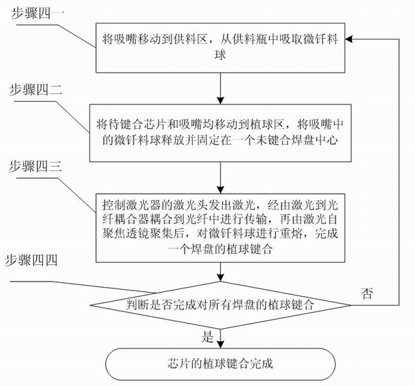
[0078] 4. Bond each pad according to the ball bonding path, specifically:

[0079] Four one: The suction nozzle 3 moves to the top of the feeding port by moving in the direction of the Zt axis and Yt axis, and then t...


PUM

PropertyMeasurementUnit
diameteraaaaaaaaaa
diameteraaaaaaaaaa
diameteraaaaaaaaaa

Abstract

The invention provides an MEMS stereoscopic packaging-assembling oriented solder ball bump bonding method, belonging to the field of packaging interaction and assembly of MEMS devices and solving the problems that the existing MEMS device package bonding technology dose not realize standardization, and the existing MEMS device automatic bonding technology is only suitable for manufacture laser bumps of specific bonding pad surfaces, can not realize integration of bump manufacture and interaction, and is not suitable for MEMS device stereoscopic packaging. The method comprises the following steps: transporting a chip to be bound to the visual system work area of an image acquiring device, acquiring image information, calculating to obtain the positions of all the bonding pad centers to be bound of the chip to be bound, storing all position information, planning bumping bonding paths based on the position information, and bonding each bonding pad based on the bumping bonding paths, wherein the bonding step is composed of sucking micro solder balls by utilizing a suction nozzle, releasing the micro solder balls into the bonding center and finishing bonding. The invention is applicable to the stereoscopic packaging of the MEMS devices.

Description

Technical field [0001] The invention relates to a solder ball bump bonding method for MEMS three-dimensional packaging and assembly, and belongs to the field of packaging interconnection and assembly of MEMS devices. Background technique [0002] Micro Electromechanical System MEMS (MicroElectromechanical System) is a combination of silicon microfabrication technology in integrated circuit IC (IntegratedCircuit) manufacturing process and micromechanical processing technology in the machinery industry by adopting the currently fast-developing high-tech technology. A new device or system that integrates even light, machine, and electricity has the characteristics of low cost, small size, low power consumption, high integration, and mass production. The structure and function of different MEMS devices are very different, and their application environments are also different, resulting in the packaging cost of MEMS devices being almost 50% to 80% of the manufacturing cost. Therefore...

Claims


Application Information

Patent Timeline
Patent Type & Authority Applications(China)
IPC IPC(8): B81C3/00
Inventor 王春青杨磊刘威田艳红
Owner HARBIN INST OF TECH
Why Eureka
Try Eureka