Method for processing through hole of printed circuit board, printed circuit board and communication equipment

A technology for printed circuit boards and processing methods, which is applied in the fields of printed circuit components, electrical connection formation of printed components, multi-layer circuit manufacturing, etc., and can solve problems such as the inability to realize signal interconnection at any layer, and the inability to separate wires from any layer at the same time.

Active Publication Date: 2009-11-18
HUAWEI TECH CO LTD
View PDF0 Cites 11 Cited by
  • Summary
  • Abstract
  • Description
  • Claims
  • Application Information

AI Technical Summary

Problems solved by technology

[0008] The prior art solution is to obtain the pressed multi-layer structure first, drill the multi-layer structure to obtain the outer layer shielding via hole, and fill the hole with insulation Medium, then drill holes to get the inner layer vias and fill in the conductors to get the coaxial via structure, so that it is impossible to realize the wiring from the same layer to any layer at the same time, that is, it is impossible to realize the signal interconnection of any layer

Method used


Image

  • Method for processing through hole of printed circuit board, printed circuit board and communication equipment
  • Method for processing through hole of printed circuit board, printed circuit board and communication equipment
  • Method for processing through hole of printed circuit board, printed circuit board and communication equipment

Examples


Embodiment 1

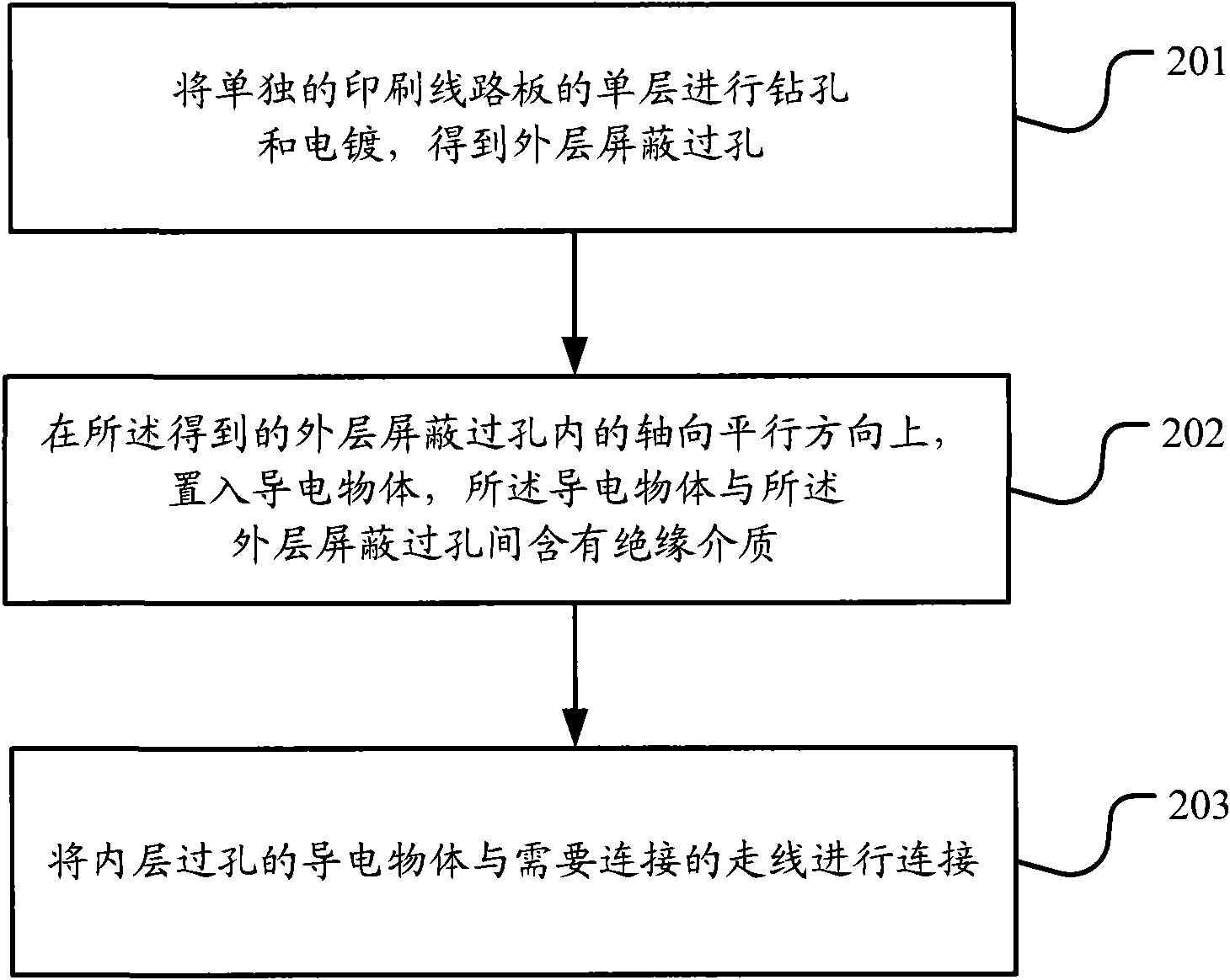
[0057] 1. Process the first layer of copper-clad board:

[0058] See Figure 5 , Is a schematic diagram of processing a pair of first-layer copper-clad boards in an embodiment of the present invention:

[0059] Steps 501-502, drilling and electroplating the copper-clad board to obtain the first metalized via, that is, the outer shielding via of the coaxial via;

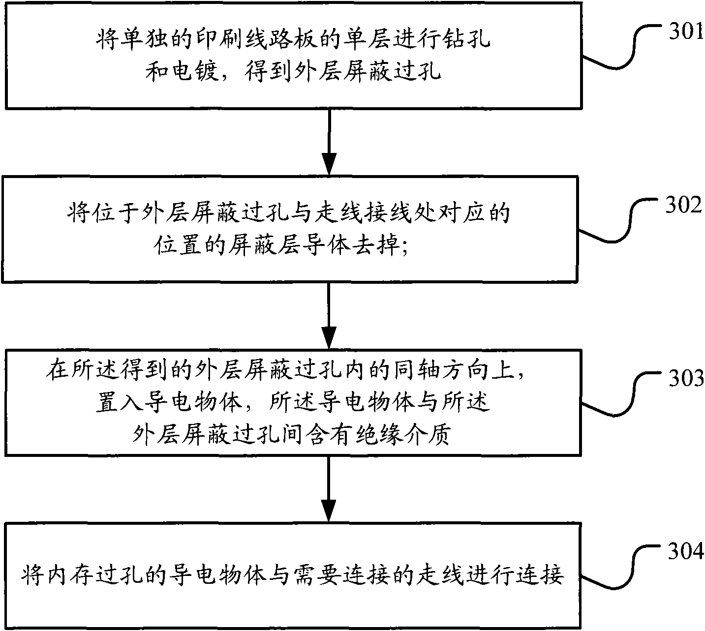
[0060] Step 503: Remove the shielding layer conductor at the position corresponding to the outer shielding via wall and the wiring connection;

[0061] For details about removing the shielding layer conductor, refer to the description in step 302 above.

[0062] It should be noted that if the coaxial inner layer via does not need to be led out of the shielding via with a wire, this step is not available. If it is necessary to use a wire to lead out of the shielding via, perform this step.

[0063] Through this step, it is ensured that the signal trace can be connected to the inner via hole in the same layer of the shieldi...

Embodiment 2

[0087] The technical solution of the second embodiment can also achieve the beneficial effects described in the first embodiment, and the implementation can be simpler by adopting the method of pressing into the conductor with insulating medium.

[0088] The following describes the third embodiment of the present invention. The technical solution of the third embodiment is basically the same as that of the first embodiment. The main difference is that after the outer shielded via hole that has been filled with an insulating medium is drilled, the newly drilled hole is not filled with a conductor. A layer of chemical copper is deposited on the wall of the newly drilled hole or a layer of metal is attached by electroplating, which also functions as a conductor. For the copper-clad board, after the inner layer via hole is drilled, it is not electroplated immediately, but after the pattern is completed, the inner layer via hole will be hollow instead of solid. For the insulating diele...

Embodiment 3

[0089]The technical solution of the third embodiment can also achieve the beneficial effects described in the first embodiment, and provides another method of filling the conductor by depositing a layer of chemical copper on the wall of the newly drilled hole or attaching a layer of metal by electroplating. the way.

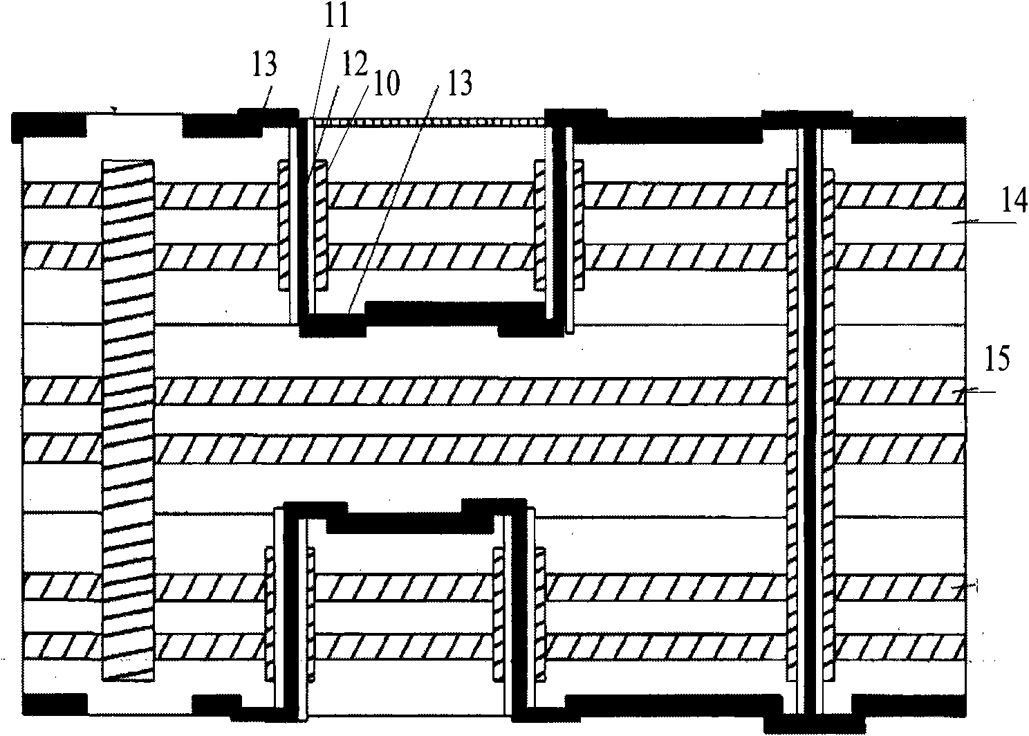
[0090] The following describes the fourth embodiment of the present invention, please refer to Figure 13 , Is a schematic diagram of alternative steps for implementing one in the fourth embodiment of the present invention. Figure 14 , Is a cross-sectional view of the central control deep borehole in the fourth embodiment of the present invention.


PUM


Abstract

The invention discloses a method for processing a through hole of a printed circuit board, a printed circuit board and communication equipment. The method comprises the following steps: a single layer of the printed circuit board confirmed to be drilled is singly processed so as to obtain a metallic outer-layer shielded through hole; a conductive body is arranged in an axial parallel direction in the obtained outer-layer shielded through hole, and an insulating medium is contained between the conductive body and the outer-layer shielded through hole; and the conductive body is connected with a confirmed cable. The printed circuit board comprises at least one single-layer board, wherein the single-layer board contains the metallic outer-layer shielded through hole; an axle centre in the outer-layer shielded through hole contains the conductive body, and the insulating medium is contained between the conductive body and the outer-layer shielded through hole; the conductive body is telecommunicated with the cable; and the position of the outer-layer shielded through hole wall, corresponding to the connecting part of the cable, contains a groove, and the insulating medium is filled in the groove. The technical scheme can lead signals at all layers in the printed circuit board to be connected with each other.

Description

Technical field [0001] The invention relates to the field of printed circuit board manufacturing, in particular to a printed circuit board via hole processing method, printed circuit board and communication equipment. Background technique [0002] In traditional multi-layer circuit boards, the signal interconnections between different layers are connected through metallized vias. The so-called metalized vias (hereinafter referred to as vias) refer to holes formed by mechanically drilling or laser burning the holes, then electroplating or using other methods to attach metal to the surface of the holes. In the multi-layer circuit boards used in high-speed interconnection, the device density is getting higher and higher, and the via pitch is getting smaller and smaller, which leads to more and more serious crosstalk. In addition, the high density makes the thickness-to-diameter ratio of the multilayer circuit board increase. , Resulting in serious impedance mismatch. To solve these ...

Claims


Application Information

Patent Timeline
Patent Type & Authority Applications(China)
IPC IPC(8): H05K3/42H05K3/46H05K1/02H05K9/00
Inventor 贾功贤周熙熙
Owner HUAWEI TECH CO LTD
Why Eureka
Try Eureka