Method for carbon nano tube to achieve vertical interconnection of upper and lower layers of conductive material

A conductive material, carbon nanotube technology, applied in the field of interconnection, can solve the problems of poor quality control of carbon nanotubes, growth temperature can not be too low, non-compliance, etc.

Inactive Publication Date: 2009-10-21
SEMICON MFG INT (SHANGHAI) CORP +1
View PDF0 Cites 11 Cited by
  • Summary
  • Abstract
  • Description
  • Claims
  • Application Information

AI Technical Summary

Problems solved by technology

Due to the preparation of carbon nanotubes by PECVD method, if the growth temperature is low (<400°C), amorphous carbon is easy to be produced, and the quality of the prepared nanotubes is very poor, that is, all current methods for preparing carbon nanotube through-hole interconnections All use methods such as PECVD or CVD to grow carbon nanotubes in-situ. First of all, the growth temperature should not be too low, so it does not meet the growth temperature lower than 400°C predicted by ITRS.
In addition, due to the on-site growth, the quality of the prepared carbon nanotubes is not easy to control

Method used


Image

  • Method for carbon nano tube to achieve vertical interconnection of upper and lower layers of conductive material
  • Method for carbon nano tube to achieve vertical interconnection of upper and lower layers of conductive material
  • Method for carbon nano tube to achieve vertical interconnection of upper and lower layers of conductive material

Examples


Embodiment 1

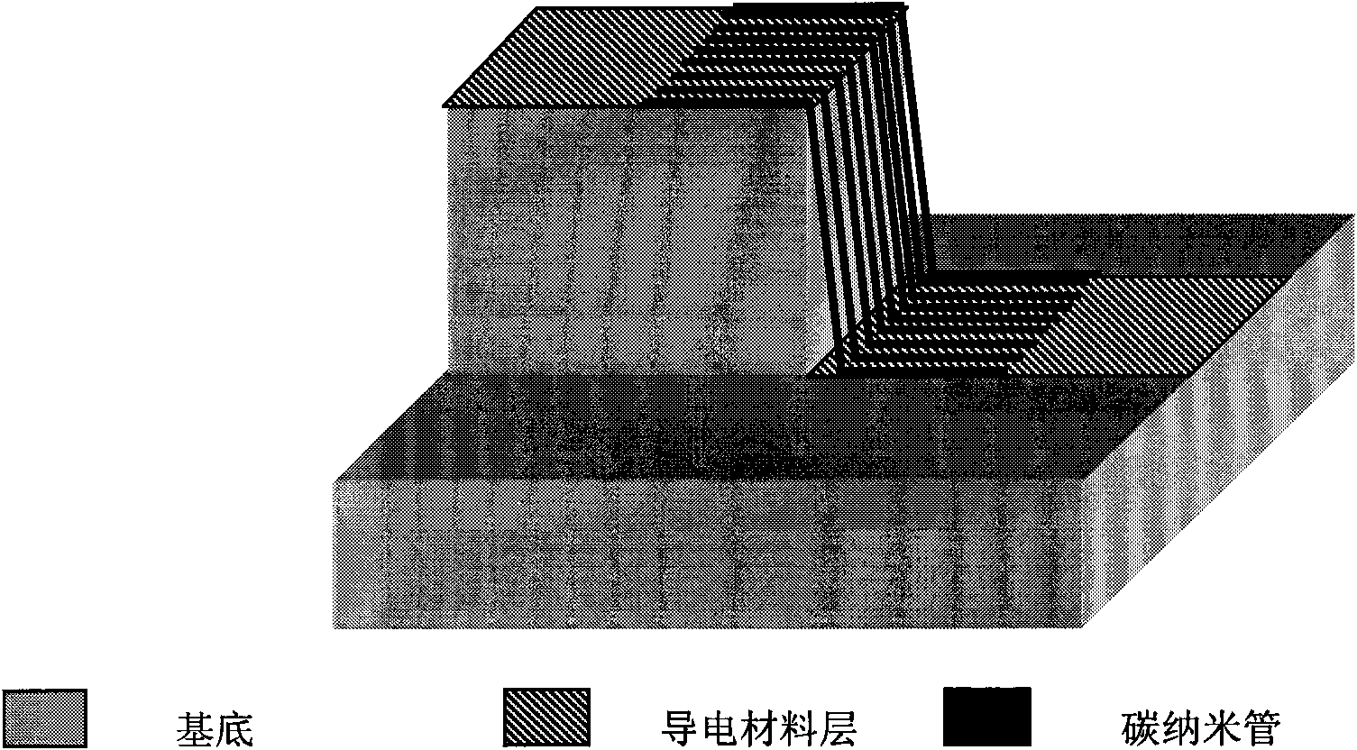
[0025] Embodiment one, with figure 1 The shown vertical structure of the boss type is taken as an example to illustrate the process of the present invention.

[0026] 1) First, etch a boss structure on the silicon substrate. There is a vertical plane between the upper surface and the lower surface of the structure. A layer of stunning dielectric layer can be deposited on the above-mentioned boss structure, such as figure 2 (a) shown.

[0027] The substrate can be a semiconductor material such as Si, Ge, GaAs, or an integrated circuit structure.

[0028] The above insulating dielectric layer can be SiO 2 , Organic, nitrogen-doped oxides or porous low-K dielectric materials.

[0029] 2) depositing a conductive layer on the vertical structure;

[0030] The upper and lower layers of conductive materials can be the same material or different materials, including but not limited to metals, highly doped semiconductor materials: Si, Ge, GaAs, carbon nanotube films or conductive p...

Embodiment 2

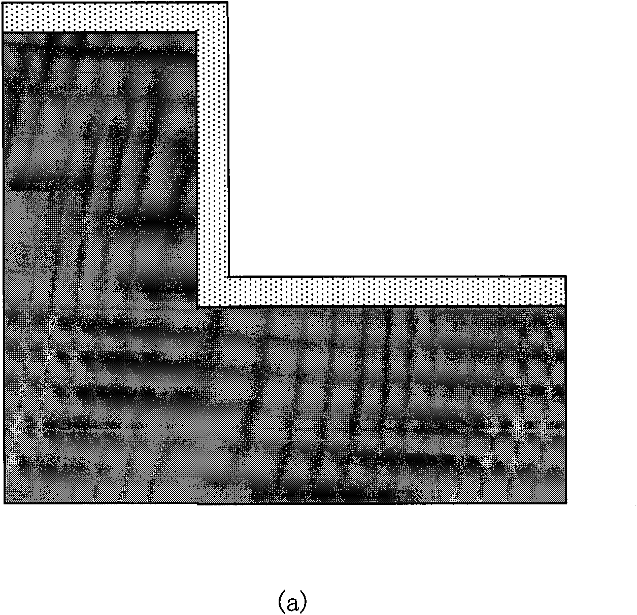
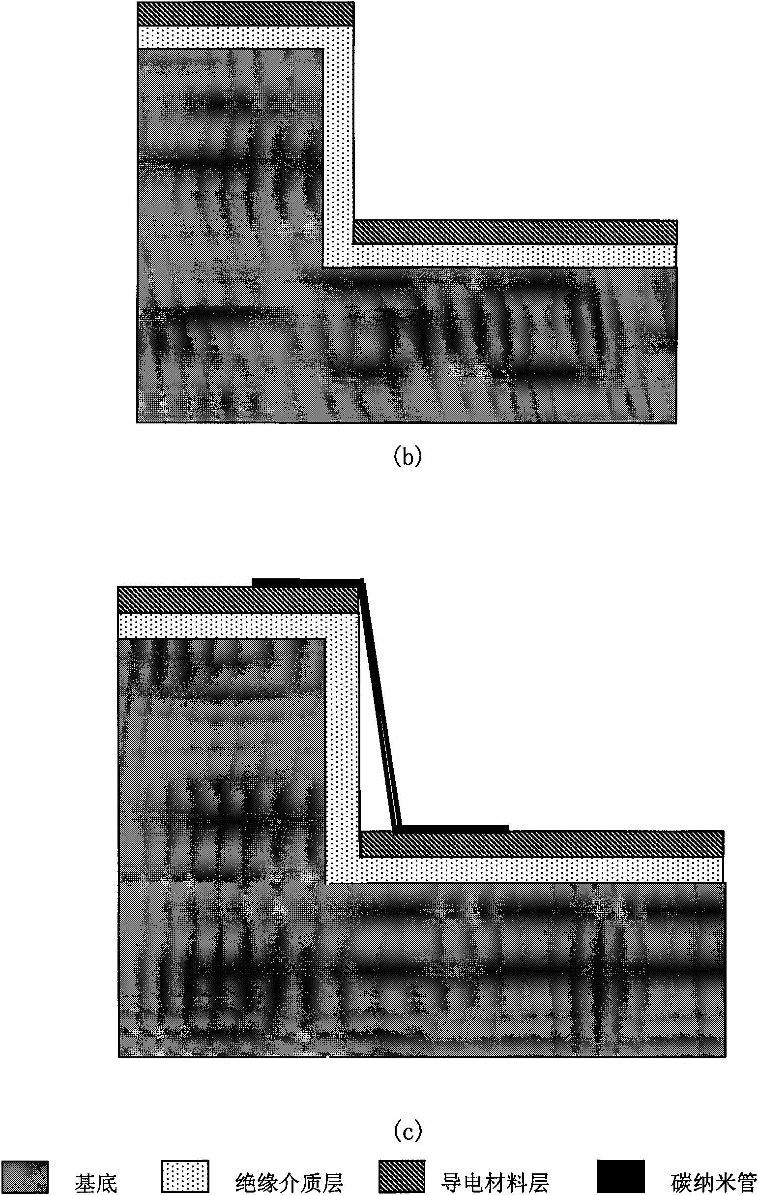
[0038] Embodiment two, with image 3 The groove-type vertical structure shown is taken as an example to illustrate the process of the present invention.

[0039] 1) First, etch a groove structure on the substrate, three vertical planes are arranged between the upper surface and the lower surface of the structure, and a layer of insulating dielectric layer can be deposited on the above-mentioned vertical structure, such as image 3 (a) shown.

[0040] The substrate can be a semiconductor material such as Si, Ge, GaAs, or any vertical structure of an integrated circuit; material 2 is an insulating dielectric material, which can be SiO 2 , Organic, nitrogen-doped oxides or porous low-K dielectric materials.

[0041] 2) Deposit a conductive layer on the upper and lower two-layer structure;

[0042] The deposited conductive layer can be metals such as Ti / Au, or highly doped semiconductor materials such as Si, Ge, GaAs, etc., as shown in 3(b).

[0043] The conductive materials o...


PUM


Abstract

The invention discloses a method for a carbon nano tube to achieve vertical interconnection of upper and lower layers of a conductive material, and belongs to the interconnection technology in an integrated circuit. The method comprises the following steps: preparing a vertical structure comprising upper and lower horizontal planes on a substrate; depositing the conductive material on the vertical structure to form upper and lower conductive layers; preparing carbon nano tube solution, dripping the carbon nano tube solution onto the vertical structure, applying direct current or alternating current between the upper and lower conductive layers, and lapping two ends of the carbon nano tube to the two conductive material layers; and depositing an insulating medium material to form a carbon nano tube through hole structure so as to achieve the vertical interconnection of the upper and lower layers of the conductive material. The preparation and assembly processes of the carbon nano tube are carried out respectively, and the assembly process is carried out at room temperature; therefore, the interconnection technology can avoid polluting a circuit chip during the preparation of the carbon nano tube, and can be compatible with the prior CMOS technology.

Description

technical field [0001] The invention relates to interconnection technology in integrated circuits, in particular to a vertical interconnection method between upper and lower layers of conductive materials. Background technique [0002] Interconnections in integrated circuits mainly include two types, one is horizontal interconnection within the same layer, and the other is vertical interconnection between different layers, that is, through holes. As the feature size of integrated circuits continues to scale down and the degree of integration continues to increase, the size of interconnect lines in integrated circuits also decreases, and the number of interconnect layers continues to increase. In integrated circuits, vertical interconnects that connect the upper and lower layers There are also more and more through holes. However, as the line width decreases, the resistivity of the traditional copper interconnection caused by grain boundary scattering and surface roughness i...

Claims


Application Information

Patent Timeline
Patent Type & Authority Applications(China)
IPC IPC(8): H01L21/768B82B3/00
Inventor 魏芹芹傅云义黄如张兴
Owner SEMICON MFG INT (SHANGHAI) CORP
Why Eureka
Try Eureka