

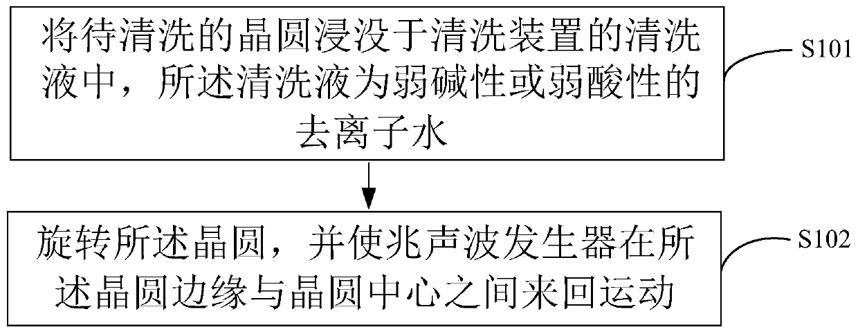
A wafer cleaning method
A wafer and cleaning liquid technology, applied in cleaning methods and tools, cleaning methods using liquids, cleaning methods using tools, etc., can solve problems such as wafer surface damage, achieve the effect of improving yield and avoiding damage
- Summary
- Abstract
- Description
- Claims
- Application Information
AI Technical Summary
Problems solved by technology
Method used
Image

Examples
Embodiment 1
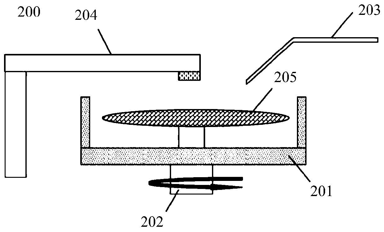
[0032] refer to figure 2 , figure 2 It is a schematic structural diagram of a wafer cleaning device in an exemplary embodiment. The wafer cleaning device 200 includes a cleaning chamber 201 , a loading platform 202 , a chemical liquid supply pipeline 203 and a megasonic generator 204 . When using the wafer cleaning device to clean the wafer, the wafer 205 is placed on the carrier table 202, the carrier table 202 rotates, the wafer 205 rotates together with the carrier table 202, and the cleaning liquid supply pipeline 203 supplies cleaning liquid to the surface of the wafer 205, The megasonic generator 204 is disposed above the surface of the wafer 205 , and the megasonic generator 204 swings above the surface of the wafer 205 .
[0033] Firstly, the wafer 205 to be cleaned is immersed in the cleaning solution of the cleaning device 200 , the cleaning solution is slightly alkaline deionized water. The wafer 205 is immersed in the cleaning solution of the cleaning device 2...
Embodiment 2
[0039] The wafer cleaning device in Embodiment 2 is the same as that in Embodiment 1, and will not be repeated here.
[0040] First, the wafer 205 to be cleaned is immersed in the cleaning solution of the cleaning device 200 , and the cleaning solution is weakly acidic deionized water. The wafer 205 is immersed in the cleaning solution of the cleaning device 200 , so the wafer 205 is in a high-pressure liquid phase environment. Preferably, the pH of the weakly acidic deionized water is 5-7, for example, hydrogenated deionized water (H2-DI) can be selected as the cleaning solution.
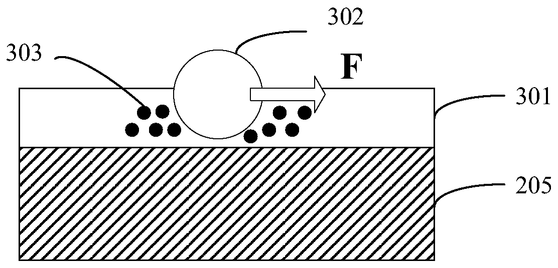
[0041]Then, the wafer 205 is rotated and the megasonic generator 204 is moved between the edge and the center of the wafer. At the same time, cleaning liquid can also be sprayed to the center of the wafer. The sprayed cleaning liquid is the same as the cleaning liquid in the cleaning device. The rotating speed range of the wafer 205 is: 2000-2500rpm / min. The above process conditions are for the...
PUM
 Abstract
Description
Claims
Application Information