
High-power LED double-layer hemispherical structure packaging technology

A packaging process and high-power technology, which is applied in the direction of semiconductor devices, electrical components, circuits, etc., can solve the problems of reducing the light extraction efficiency of packaging, the quantum efficiency of phosphor powder, and affecting the lumen efficiency of packaging, so as to solve the problem of quantum efficiency decline and cost Low, good convergence effect

Active Publication Date: 2018-05-08
XIAN CREATION KEJI CO LTD
View PDF5 Cites 1 Cited by
  • Summary
  • Abstract
  • Description
  • Claims
  • Application Information

AI Technical Summary

Problems solved by technology

Since the chip absorbs the backscattered light, this direct coating method will reduce the light extraction efficiency of the package
In addition, if the phosphor is directly coated on the chip, the high temperature generated by the chip will significantly reduce the quantum efficiency of the phosphor, which will seriously affect the lumen efficiency of the package.

Method used


Image

  • High-power LED double-layer hemispherical structure packaging technology
  • High-power LED double-layer hemispherical structure packaging technology
  • High-power LED double-layer hemispherical structure packaging technology

Examples


Embodiment 1

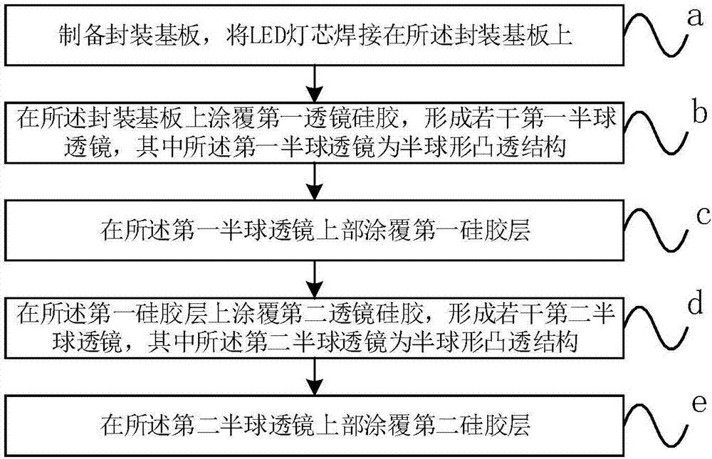
[0050] figure 1 A flow chart of a high-power LED double-layer hemispherical structure packaging process provided by an embodiment of the present invention includes the following steps:

[0051] a. Prepare the package heat dissipation substrate, and weld the LED wick on the package heat dissipation substrate;

[0052] b. Coating the first lens silica gel on the package heat dissipation substrate to form a plurality of first hemispherical lenses, wherein the first hemispherical lenses are hemispherical convex structures;

[0053] c. Coating a first silica gel layer on the top of the first hemispherical lens;

[0054] d. Coating second lens silica gel on the first silica gel layer to form a plurality of second hemispherical lenses, wherein the second hemispherical lenses are hemispherical convex structures;

[0055] e. Coating a second silica gel layer on the upper part of the second hemispherical lens;

[0056] Wherein, at least one of the second hemispherical lens and the se...


PUM


Abstract

The invention relates to a high-power LED double-layer hemispherical structure packaging technology, which comprises the following steps of (a) preparing a packaging heat dissipation substrate and welding an LED lamp core on the packaging heat dissipation substrate; (b) coating the packaging heat dissipation substrate with first lens silica gel and forming a plurality of first hemispherical lenses, wherein the first hemispherical lenses are of a hemispherical convex lens structure; (c) coating the upper parts of the first hemispherical lenses with a first silica gel layer; (d) coating the first silica gel layer with second lens silica gel and forming a plurality of second hemispherical lenses, wherein the second hemispherical lenses are of a hemispherical convex lens structure; and (e) coating the upper parts of the second hemispherical lenses with a second silica gel layer, wherein at least one layer of the second hemispherical lenses and the second silica gel layer contains fluorescent powder and the LED lamp core is an ultraviolet lamp core. According to the high-power LED double-layer hemispherical structure packaging technology, secondary shaping is not needed, so that the technology is simple and the cost is low.

Description

technical field [0001] The invention belongs to the field of semiconductor packaging, and in particular relates to a high-power LED double-layer hemispherical structure packaging process. Background technique [0002] A light-emitting diode (English: Light-Emitting Diode, referred to as LED) is a semiconductor electronic component that can convert electrical energy into light energy. With the continuous development of the industry, breakthroughs in technology, and vigorous promotion of applications, the light efficiency of LEDs is also constantly improving. The improvement of the control software also makes the use of LED lighting more convenient. These gradual changes all reflect the broad prospects of LED light-emitting diodes in lighting applications. It has the characteristics of energy saving, environmental protection, safety, long life, low power consumption, low heat, high brightness, waterproof, miniature, shockproof, easy dimming, concentrated beam, easy maintenan...

Claims


Application Information

Patent Timeline
Patent Type & Authority Applications(China)
IPC IPC(8): H01L33/62H01L33/64H01L33/50H01L33/58
CPCH01L33/502H01L33/58H01L33/62H01L33/64
Inventor 左瑜
Owner XIAN CREATION KEJI CO LTD
Learn More