Camera module package process and structure

A camera module, packaging technology, applied in image communication, TV, color TV components and other directions, can solve problems such as easy pollution, reflected energy, refraction, etc.

Inactive Publication Date: 2018-05-08
TRULY OPTO ELECTRONICS
View PDF7 Cites 12 Cited by
  • Summary
  • Abstract
  • Description
  • Claims
  • Application Information

AI Technical Summary

Problems solved by technology

[0002] At present, there are two main production processes for camera modules. One is the COB process, which uses bare chip packaging. The bare chip is fragile and easily contaminated. The process is very difficult to control and the production yield is low, so it is currently difficult to Really achieve mass production; the other is the CSP process, which adds a packaging layer on the bare chip, but due to slight refraction, reflection and energy loss when light penetrates the packaging layer, its image effect is not directly used with the bare chip. The module made by advanced COB technology has good effect

Method used


Image

  • Camera module package process and structure
  • Camera module package process and structure
  • Camera module package process and structure

Examples


Embodiment Construction

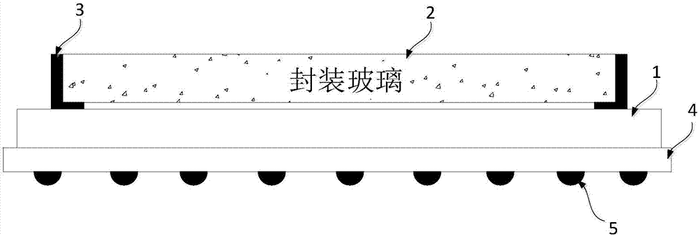
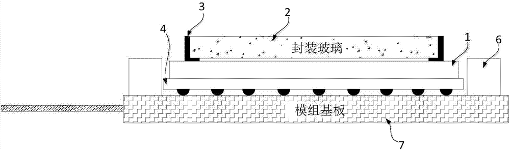
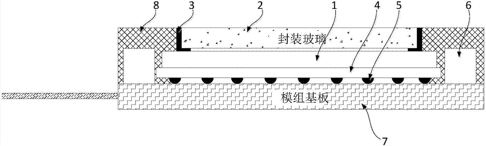
[0032] The first object of the present invention is to provide a camera module package structure, the structural design of the camera module package structure can reduce the risk of contamination of the bare chip, so as to facilitate process control, improve the yield rate, and at the same time ensure the quality of the camera module. To influence the effect, the second object of the present invention is to provide a camera module packaging structure based on the above camera module packaging process.

[0033] The following will clearly and completely describe the technical solutions in the embodiments of the present invention with reference to the accompanying drawings in the embodiments of the present invention. Obviously, the described embodiments are only some, not all, embodiments of the present invention. Based on the embodiments of the present invention, all other embodiments obtained by persons of ordinary skill in the art without making creative efforts belong to the p...


PUM


Abstract

The invention discloses a camera module package process and structure. The package process comprises the following steps: sticking a package layer on a photosensitive region of a photosensitive chip in degradable mucilage glue; connecting the photosensitive chip and the component to a module substrate; injection-molding an annular plastic layer on the module substrate, wrapping the component in the plastic layer and wrapping the photosensitive chip from the circumference; degrading the degradable mucilage glue, and peeling off the package layer from the photosensitive region of the photosensitive chip; clearing the degradable mucilage glue, and loading an optical filter and a lens on the annular plastic layer. Through the adoption of the above process, the package layer is firstly stuck onthe photosensitive chip by using the degradable mucilage glue, thereby preventing the photosensitive region of the photosensitive chip from being polluted in the subsequent manufacturing procedure, and achieving the aims of facilitating manufacturing procedure control and improving the yield; after the module semi-finished product is completely manufactured, namely, after the annular plastic injection-molding is finished and the optical filter and the lens are loaded, the package layer is peeled off from the photosensitive region, thereby preventing the package layer from causing light ray refraction, reflection and energy loss, and achieving an aim of improving the image effect.

Description

technical field [0001] The invention relates to the technical field of camera module packaging, in particular to a camera module packaging process and structure. Background technique [0002] At present, there are two main production processes for camera modules. One is the COB process, which uses bare chip packaging. The bare chip is fragile and easily contaminated. The process is very difficult to control and the production yield is low, so it is currently difficult to Really achieve mass production; the other is the CSP process, which adds a packaging layer on the bare chip, but due to slight refraction, reflection and energy loss when light penetrates the packaging layer, its image effect is not directly used with the bare chip. The module made by advanced COB technology has good effect. [0003] Therefore, how to improve the current module manufacturing process so that it can reduce the risk of bare chip contamination, facilitate process control, improve yield, and at ...

Claims


Application Information

Patent Timeline
Patent Type & Authority Applications(China)
IPC IPC(8): H04N5/225
CPCH04N23/50H04N23/54H04N23/55
Inventor 韦有兴李建华
Owner TRULY OPTO ELECTRONICS
Why Eureka
Try Eureka