Flexible circuit board and display device

A flexible circuit board and electrical connection technology, which is applied in the direction of circuit devices, printed circuits, printed circuits, etc., can solve the problems of reduced soldering yield, poor soldering, alignment deviation of flexible circuit boards, etc., to reduce electromagnetic interference And electrostatic interference, improve the quality of signal transmission, improve the effect of welding accuracy

Active Publication Date: 2018-05-08
WUHAN TIANMA MICRO ELECTRONICS CO LTD
View PDF3 Cites 11 Cited by
  • Summary
  • Abstract
  • Description
  • Claims
  • Application Information

AI Technical Summary

Problems solved by technology

However, due to the problem of alignment accuracy, flexible circuit boards and other circuit boards are prone to alignment deviation, resulting in poor soldering and reduced soldering yield
[0004] In addition, flexible circuit boards are generally made of base film made of polyimide or polyester film, copper foil and cover film through bonding glue, and some alignment marks are usually removed during the preparation process. Divide the copper foils that were originally connected together into copper foils that are not connected to each other, thereby destroying the integrity of the copper foil connection and reducing the anti-electromagnetic interference ability of the flexible circuit board
The copper foil of the flexible circuit board is usually grounded, and the destruction of the electrical connection integrity of the copper foil will further reduce the anti-static interference ability of the flexible circuit board, thereby affecting the normal operation of the signal lines and wiring circuits on the flexible circuit board

Method used


Image

  • Flexible circuit board and display device
  • Flexible circuit board and display device
  • Flexible circuit board and display device

Examples


Embodiment Construction

[0031] The following will clearly and completely describe the technical solutions in the embodiments of the present invention with reference to the drawings in the embodiments of the present invention.

[0032] It should be noted that in the following description, specific details are set forth in order to fully understand the present invention. However, the present invention can be implemented in many other ways than those described here, and those skilled in the art can make similar extensions without departing from the connotation of the present invention. Accordingly, the present invention is not limited to the specific embodiments disclosed below.

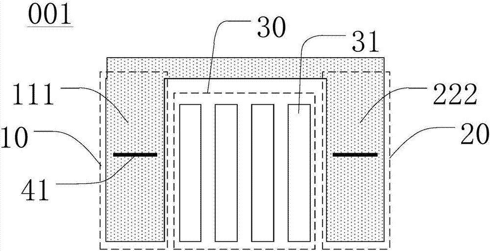
[0033] The invention relates to a flexible circuit board and a display device, figure 1 It is a structural schematic diagram of a flexible circuit board provided by the prior art. The flexible circuit board 001 includes a pad area 30, a plurality of pads 31 are arranged in the pad area 30, a first copper foil area 10 and a s...


PUM


Abstract

The present invention provides a flexible circuit board and a display device. The flexible circuit board comprises a pad area and copper foil areas at both sides. Each copper foil area comprises two subsidiary copper foil areas and an alignment mark area, each alignment mark area comprises an alignment mark and a connecting structure, and each connecting structure electrically connects subsidiarycopper foils of the two corresponding subsidiary copper foil areas. The Orthographic projections of the alignment mark of each alignment mark area and the corresponding connecting structure on the flexible circuit board are not overlapped. The technical scheme can improve the welding precision of the flexible circuit board and other components and keep the integrity of the electrical connection ofthe copper foils, so that electrostatic interference signals and electromagnetic interference signals produced in the installing or working process of the flexible circuit board are timely conductedinto a grounding wire and eliminated, the problem that the interference signals affect the normal operation of the other components of the flexible circuit board or signal lines is avoided, and thus the signal transmission quality of the flexible circuit board is improved.

Description

technical field [0001] The invention relates to the field of display technology, in particular to a flexible circuit board and a display device. Background technique [0002] Flexible circuit boards are widely used in the field of display technology because they can be bent, folded, and flexibly arranged according to the installation space. With the development of electronic products in the direction of lighter, smaller and thinner, and the complexity of product functions, higher requirements are placed on the accuracy of soldering other devices on flexible circuit boards. [0003] The flexible circuit board is usually provided with pads for welding with other circuit boards as connection ports. During the welding process, it is necessary to weld according to the alignment marks. However, due to the problem of alignment accuracy, flexible circuit boards and other circuit boards are prone to alignment deviation, resulting in poor soldering and reduced soldering yield. [0...

Claims


Application Information

Patent Timeline
Patent Type & Authority Applications(China)
IPC IPC(8): H05K1/02
CPCH05K1/0218H05K1/0266H05K2201/09818
Inventor 廖引刘敏谭绿水陈浩
Owner WUHAN TIANMA MICRO ELECTRONICS CO LTD
Why Eureka
Try Eureka