Semiconductor device aging experiment equipment and method

The technology of an experimental device and experimental method, which is applied in the field of mature experimental devices for semiconductor devices, can solve the problems of mature semiconductor devices and failure to meet standard requirements, and achieve complete screening and assessment, huge market potential, and broad economic benefits.

Inactive Publication Date: 2018-05-11
朝阳微电子科技股份有限公司
View PDF7 Cites 0 Cited by
  • Summary
  • Abstract
  • Description
  • Claims
  • Application Information

AI Technical Summary

Problems solved by technology

[0005] The technical problem mainly solved by the present invention is to provide a semiconductor device aging device and method, which can fundamentally solve the problem that semiconductor device aging cannot meet the standard requirements, and can effectively improve the reliability index of semiconductor devices

Method used


Image

  • Semiconductor device aging experiment equipment and method
  • Semiconductor device aging experiment equipment and method
  • Semiconductor device aging experiment equipment and method

Examples


Embodiment Construction

[0017] The specific embodiment of the present invention is described below in conjunction with accompanying drawing:

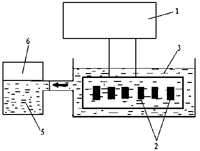
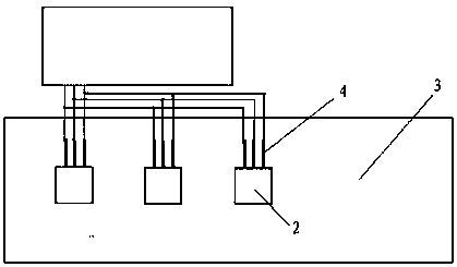
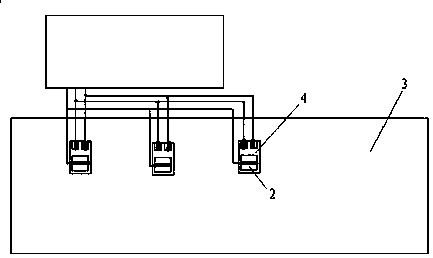
[0018] Such as figure 1 As shown, the semiconductor device aging experiment device provided by the present invention includes an aging power supply system 1, a semiconductor device 2, an oil tank 3, a clamp 4, and a cooling system. The semiconductor device 2 is clamped by the clamp 4 and placed in the oil tank 3. The semiconductor device 2 It is electrically connected with the aging power system 1, the cooling system is used to control the oil temperature and the junction temperature of the semiconductor device, and the clamp 4 is used for fixing and electrically connecting the semiconductor device 2, including figure 2 shown in the TO series and image 3 Two TMD series products are shown.

[0019] Preferably, the semiconductor devices 2 can be connected in parallel or in series as required.

[0020] Preferably, the cooling system includes a control system...


PUM


Abstract

The invention particularly relates to semiconductor device aging experiment equipment and a semiconductor device aging experiment method, and belongs to the technical field of semiconductor device processing technology. The invention aims to provide semiconductor device aging equipment and a method thereof, wherein the problem that the standard requirement cannot be met by the aging of semiconductor devices in the prior art can be fundamentally solved. The equipment comprises an aging power supply system, a semiconductor device, an oil tank, a clamp and a cooling system. The semiconductor device is clamped by the clamp and is arranged in the oil tank. The semiconductor device is electrically connected with the aging power supply system. The cooling system is used for controlling the temperature of the oil and the junction temperature of the semiconductor device. The method comprises the steps of placing the semiconductor device in the oil tank through the impregnation method, accurately controlling the temperature of the oil and the junction temperature of the semiconductor device through the cooling system, and realizing the aging function of the semiconductor device. According tothe invention, multiple devices (100-200 devices) can be aged through one shot by designing an aging test bed. Therefore, the working efficiency of aging is greatly improved.

Description

technical field [0001] The invention specifically relates to a semiconductor device aging experiment device and method, and belongs to the technical field of semiconductor device processing. Background technique [0002] Existing semiconductor device aging test benches use air cooling and water cooling to control the junction temperature of the device. The device is connected to the heat sink through a sophisticated fixture, and the thermal resistance is reduced through close contact between the device shell and the heat sink. The heat generated by the device chip is directly transmitted to the heat sink through the tube shell, and the heat sink transmits the heat to the ambient air through air cooling or water cooling, so as to achieve the purpose of heat transfer. The shell and the heat sink are matched by crimping. Due to the unevenness of the two end faces, it is difficult to ensure a complete match of the contact interface, and the application of thermal grease will af...

Claims


Application Information

Patent Timeline
Patent Type & Authority Applications(China)
IPC IPC(8): G01R31/26
CPCG01R31/2601
Inventor 李志福
Owner 朝阳微电子科技股份有限公司
Why Eureka
Try Eureka