Conductive material and connecting structure
A technology of conductive materials and conductive particles, applied in conductive materials, conductive materials, conductors, etc., can solve problems such as reduced conductivity reliability
- Summary
- Abstract
- Description
- Claims
- Application Information
AI Technical Summary
Problems solved by technology
Method used
Image
Examples
Embodiment 1~17 and comparative example 1~2
[0299] (1) Preparation of anisotropic conductive paste
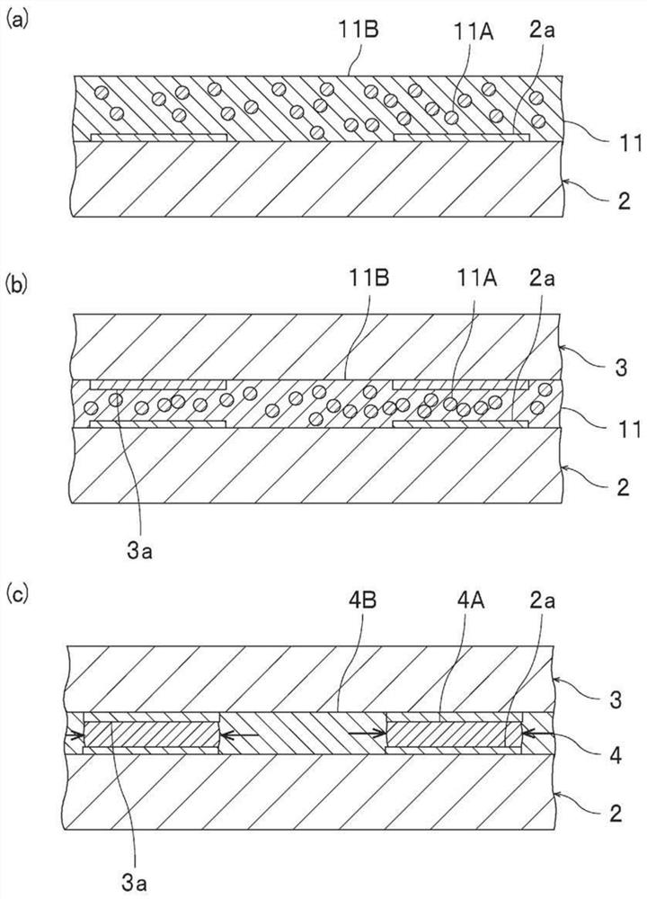
[0300] The components shown in the following Table 1 and Table 2 were compounded in the compounding quantities shown in the following Table 1 and Table 2, and the anisotropic conductive paste was obtained. In the obtained anisotropic conductive paste, the flux was present in the states shown in Tables 1 and 2.
[0301] (2) Fabrication of connection structure (array)
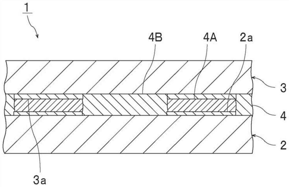
[0302] The following semiconductor chip was prepared as the first connection target part: Copper electrodes with a diameter of 250 μm and a thickness of 10 μm were arranged in an array on the surface of the semiconductor chip body (5×5 mm in size and 0.4 mm in thickness) at a pitch of 400 μm. The number of copper electrodes was 10×10 per semiconductor chip, 100 in total.
[0303] Prepare the following glass epoxy substrate as the second connection object part: On the surface of the glass epoxy substrate main body (size 20×20mm, thickness 1.2mm, material F...
PUM
| Property | Measurement | Unit |
|---|---|---|
| particle size | aaaaa | aaaaa |
| melting point | aaaaa | aaaaa |
| particle size | aaaaa | aaaaa |
Abstract
Description
Claims
Application Information


