Separated type near-field micro-nano photoetching method and device based on white light interferometry gap detection and ultraprecise aligned overlaying technology

An overlay technology, a white light interference technology, is applied in the field of separate near-field micro-nano lithography methods and devices, and can solve the problems of large lateral displacement of the reticle and the substrate, short service life of the reticle, and low alignment accuracy, etc. Achieve the effect of improving service life, improving accuracy, ensuring stability and reliability

Inactive Publication Date: 2018-05-15
INST OF OPTICS & ELECTRONICS - CHINESE ACAD OF SCI
View PDF5 Cites 8 Cited by
  • Summary
  • Abstract
  • Description
  • Claims
  • Application Information

AI Technical Summary

Problems solved by technology

[0005] The technical problem to be solved in the present invention is to overcome the short service life of the reticle, large lateral displacement after contact between the reticle and the substrate, and low alignment accuracy in the existing near-field lithography method in the contact exposure mode. For the deficiencies, a separate near-field micro-nano lithography method and device based on white light interference gap detection and ultra-precision alignment overlay technology are provided. Closed-loop feedback control of gap detection system and alignment module realizes separate exposure and ultra-precise alignment overlay functions

Method used


Image

  • Separated type near-field micro-nano photoetching method and device based on white light interferometry gap detection and ultraprecise aligned overlaying technology
  • Separated type near-field micro-nano photoetching method and device based on white light interferometry gap detection and ultraprecise aligned overlaying technology
  • Separated type near-field micro-nano photoetching method and device based on white light interferometry gap detection and ultraprecise aligned overlaying technology

Examples


Embodiment Construction

[0058] In order to make the purpose, technical solution, device and other advantages of the present invention clearer, the present invention will be described in detail below in conjunction with the accompanying drawings and specific embodiments. However, the following embodiments are only limited to explain the present invention, and the protection scope of the present invention should include the entire contents of the claims, and through the following embodiments, those skilled in the art can realize the entire contents of the claims of the present invention.

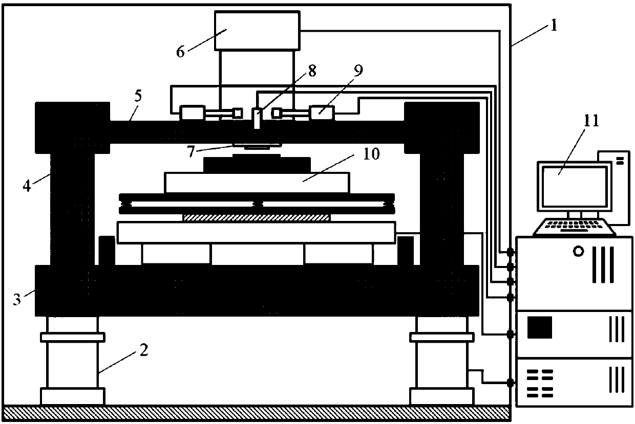
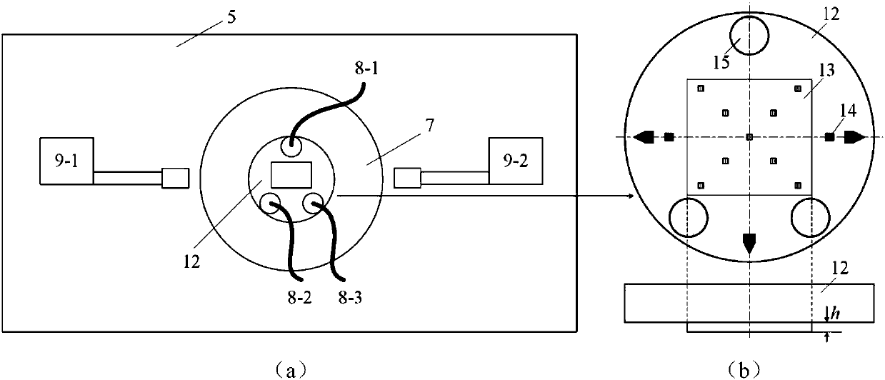
[0059] refer to figure 1 , the separated near-field micro-nano lithography device based on white light interference gap detection and ultra-precision alignment overlay technology consists of an ultra-precision environmental control system 1, an active vibration isolation platform 2, a marble plate 3, a support frame 4, and a main substrate 5 , ultraviolet exposure light source 6, lithography lens module 7, gap detect...


PUM

PropertyMeasurementUnit
heightaaaaaaaaaa
heightaaaaaaaaaa

Abstract

The invention discloses a separated type near-field micro-nano photoetching method and a device based on white light interferometry gap detection and an ultraprecise aligned overlaying technology. Themethod can achieve large-area separated type exposure and ultraprecise aligned overlaying. The device comprises an ultraprecise environmental control system, an active vibration isolation platform, asupporting framework, an ultraviolet exposure light source, a photoetching camera lens module, a gap detection system, an alignment module, a wafer chuck module and a control system. By means of a white light interference spectral measurement technology, the device can achieve nanoscale online gap detection and leveling; thus, separated type exposure is achieved; by means of the alignment moduleand the control system, the ultraprecise aligned overlaying technology can be achieved.

Description

technical field [0001] The present invention relates to the field of near-field micro-nano lithography processing technology, more specifically, to a separate near-field micro-nano lithography method and device based on white light interference precision gap detection and ultra-precision alignment overlay technology, which can realize separation super-resolution micro-nano lithography. Background technique [0002] With the rapid development of the IC industry, the miniaturization and storage density of electronic product integrated circuits are getting higher and higher, so it is urgent to develop processing technologies and equipment with high efficiency, low cost, large area and good controllability. At present, in the traditional microfabrication technology route, micron-scale processing equipment represented by laser direct writing, near-contact ultraviolet lithography, and reactive ion beam etching have been widely used in research units. Writing and focusing ion beam...

Claims


Application Information

Patent Timeline
Patent Type & Authority Applications(China)
IPC IPC(8): G03F7/20G03F9/00
CPCG03F7/2004G03F7/70483G03F7/70808G03F9/7023G03F9/7034G03F9/7038
Inventor 罗先刚龚天诚赵承伟王长涛刘玲张健刘凯鹏
Owner INST OF OPTICS & ELECTRONICS - CHINESE ACAD OF SCI
Why Eureka
Try Eureka