

Light splitter light splitting-based SP simulation lighting super-resolution photoetching lens and device
A technology for exciting illumination and spectroscope, applied in the field of super-resolution lithography, can solve the problem that the lithography device cannot meet the needs of super-resolution lithography, and achieve the effect of convenient exchange
- Summary
- Abstract
- Description
- Claims
- Application Information
AI Technical Summary
Problems solved by technology
Method used
Image

Examples
Embodiment Construction
[0049] In order to make the purpose, technical solution and advantages of the device of the present invention clearer, the present invention will be further described in detail below in conjunction with the accompanying drawings.
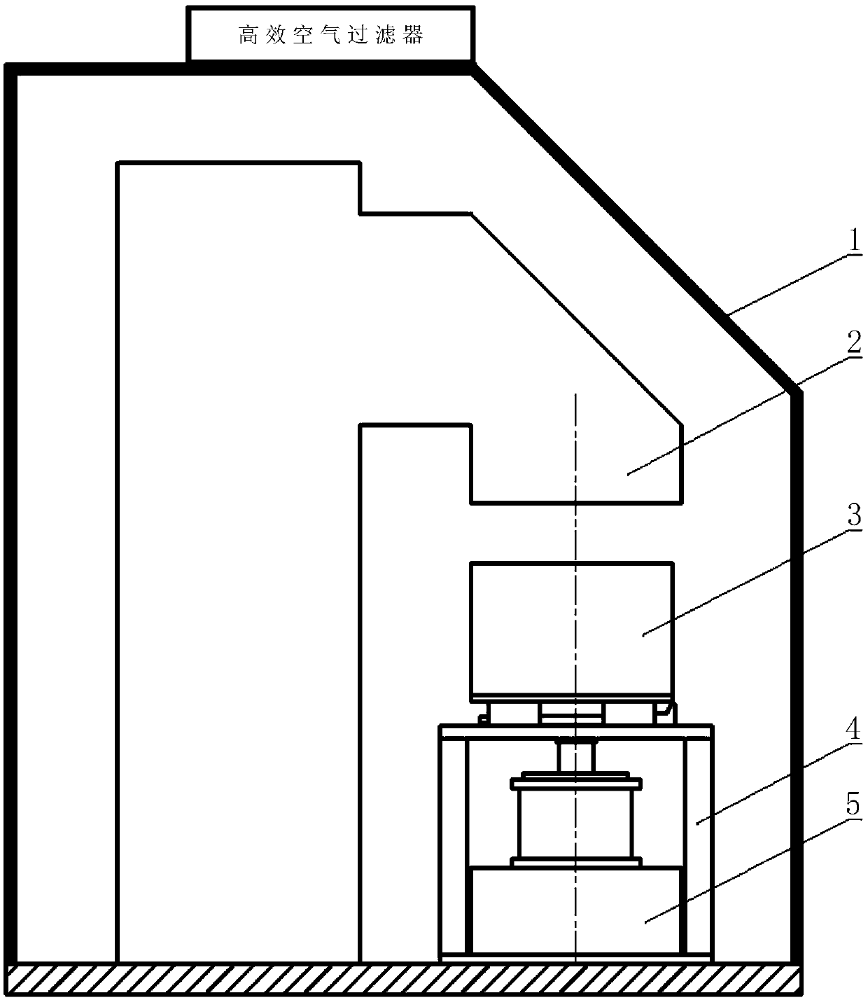
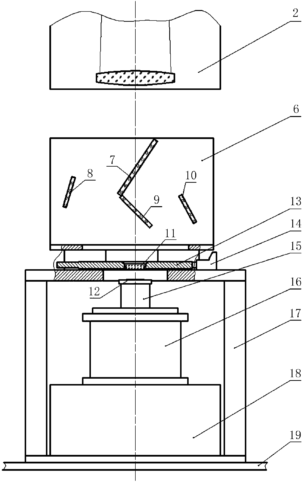
[0050] refer to figure 1 , a SP excitation illumination super-resolution lithography device based on beam splitting, the device includes an air purification system 1 for protecting the lithography device, a light source 2 for generating i-line ultraviolet exposure light beams, and a spectrophotometer for excitation illumination A mirror beam splitting system 3, a mask carrying module 4 for carrying a surface plasmon imaging device, and a workbench 5 for carrying a substrate. Among them, the air purification system 1 can ensure a good lithography environment on the one hand, and on the other hand, it is beneficial to the maintenance of the lithography device; the light source 2 provides the i-line ultraviolet exposure beam for the entire lithography ...
PUM
 Abstract
Description
Claims
Application Information