OLED substrate recognition system and method

An identification system and identification method technology, applied in the field of OLED substrate identification system, can solve problems such as substrate or program misuse, substrate and panel to be tested, substrate type mismatch, etc., to eliminate damage and avoid wrong connections.

Active Publication Date: 2018-05-18
SUZHOU HUAXING YUANCHUANG TECH CO LTD
View PDF5 Cites 1 Cited by
  • Summary
  • Abstract
  • Description
  • Claims
  • Application Information

AI Technical Summary

Problems solved by technology

[0004] At the inspection site, when the type of OLED panel to be inspected is frequently switched, sometimes due to various factors above, the substrate or program is accidentally misused, resulting in a mismatch between the host program and the external substrat

Method used


Image

  • OLED substrate recognition system and method
  • OLED substrate recognition system and method
  • OLED substrate recognition system and method

Examples


Embodiment Construction

[0034] In order to illustrate the present invention more clearly, the present invention will be further described below in conjunction with preferred embodiments and accompanying drawings. Similar parts in the figures are denoted by the same reference numerals. Those skilled in the art should understand that the content specifically described below is illustrative rather than restrictive, and should not limit the protection scope of the present invention.

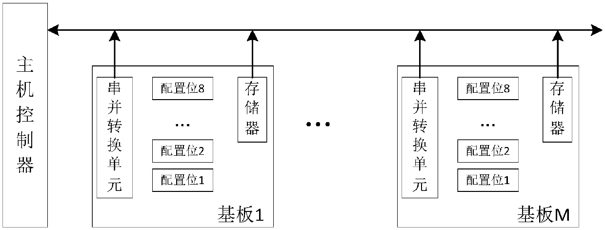
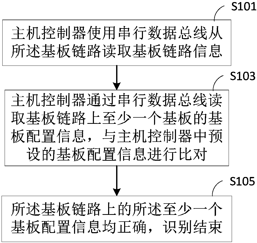
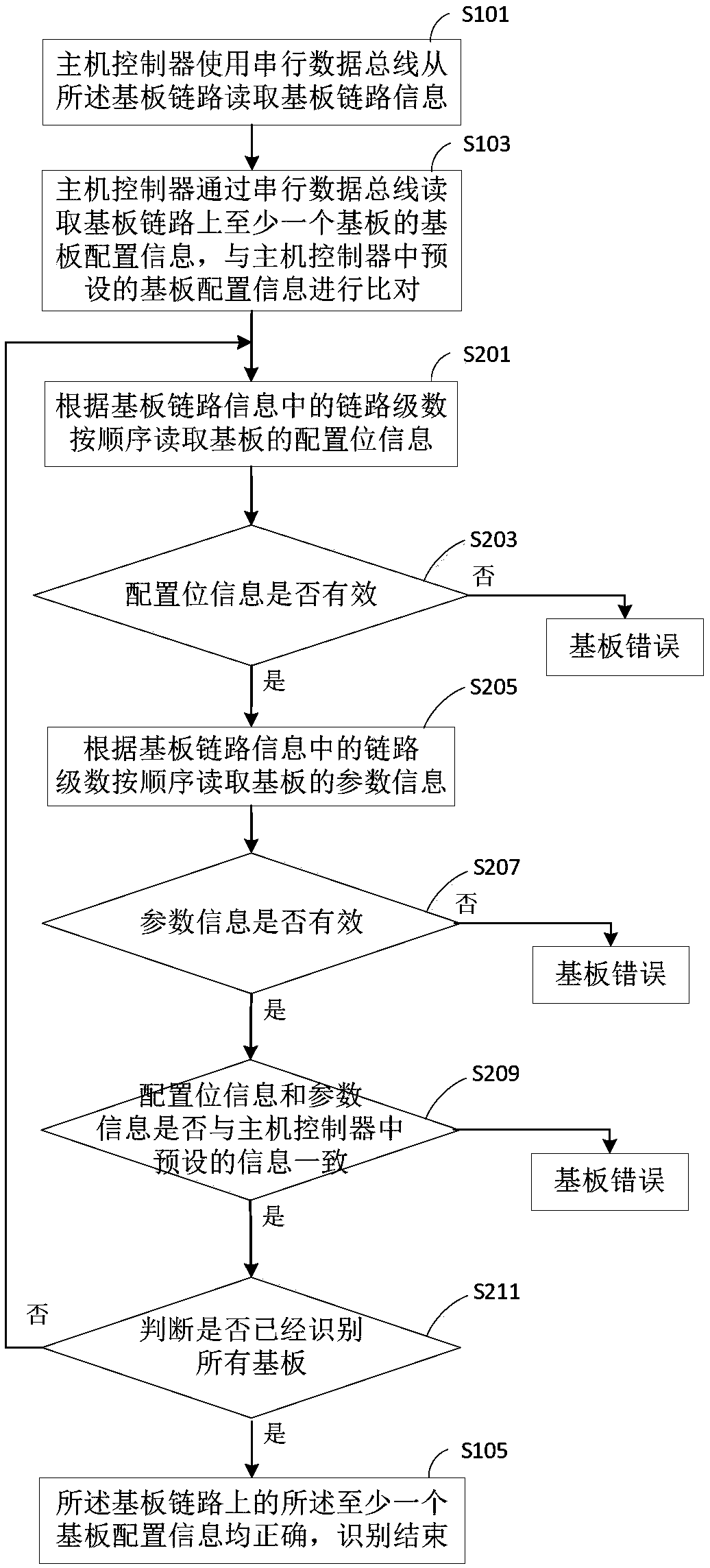
[0035] like figure 1 As shown, an embodiment of the present invention provides an OLED substrate identification system, including: a host controller, a serial data bus and at least one substrate, the host controller, the serial data bus and the at least one substrate constitute A substrate link, wherein the host controller uses the serial data bus to read the substrate link information, and reads the information on the substrate link through the serial data bus according to the substrate link information. For the substrat...


PUM


Abstract

The invention discloses an OLED substrate recognition system. The system comprises a host controller, a serial data bus and at least one substrate. The host controller, the serial data bus and the atleast one substrate form a substrate link, wherein the The host controller reads substrate link information through the serial data bus and reads substrate configuration information of the at least one substrate on the substrate link through the serial data bus according to the substrate link information, comparing the configuration information of each substrate with the substrate configuration information preset in the host controller, and outputting results. The embodiment of the invention provides the OLED substrate recognition system and method, on-line identification of a link substrate for driving an OLED panel can be achieved, and an invalid test caused by a mismatch between the substrate and a test program during an OLED panel test process and the damage of the substrate or the panel to be tested caused by a false test are avoided, so that panel test efficiency is improved.

Description

technical field [0001] The invention relates to the field of display technology, in particular to an OLED substrate identification system and method. Background technique [0002] In the current organic light-emitting diode (Organic Light-Emitting Diode, OLED) panel inspection, in order to meet the requirements of generalization and modularization, the screen and timing generation part are usually designed as a general-purpose host, leaving high-density connectors as external Interface, according to the test requirements of different types, interface types, timing, electrical parameters and other test requirements of the OLED panel to be tested, use different host programs, and replace the corresponding type of ROM substrate to generate corresponding driving signals. Connect the substrate, etc., to the OLED panel to be tested for panel testing. [0003] With the increase in the types of OLED panels tested, more and more types of ROM substrates and extension substrates are u...

Claims


Application Information

Patent Timeline
IPC IPC(8): G06F13/10
CPCG06F13/102
Inventor 陈文源陆跟成张可可丁成聪
Owner SUZHOU HUAXING YUANCHUANG TECH CO LTD
Why Eureka
Try Eureka