
Image sensor

An image sensor and photosensitive chip technology, applied in the field of sensors, can solve problems such as signal attenuation and distortion, and achieve the effect of preventing signal distortion

Pending Publication Date: 2018-06-05
WEIHAI HUALING OPTO ELECTRONICS CO LTD
View PDF14 Cites 0 Cited by
  • Summary
  • Abstract
  • Description
  • Claims
  • Application Information

AI Technical Summary

Problems solved by technology

[0008] The embodiment of the present invention provides an image sensor to at least solve the technical problem of signal attenuation and distortion caused by lengthening circuit boards and splicing circuit boards in large CISs in the prior art

Method used


Image

  • Image sensor
  • Image sensor
  • Image sensor

Examples


Embodiment 1

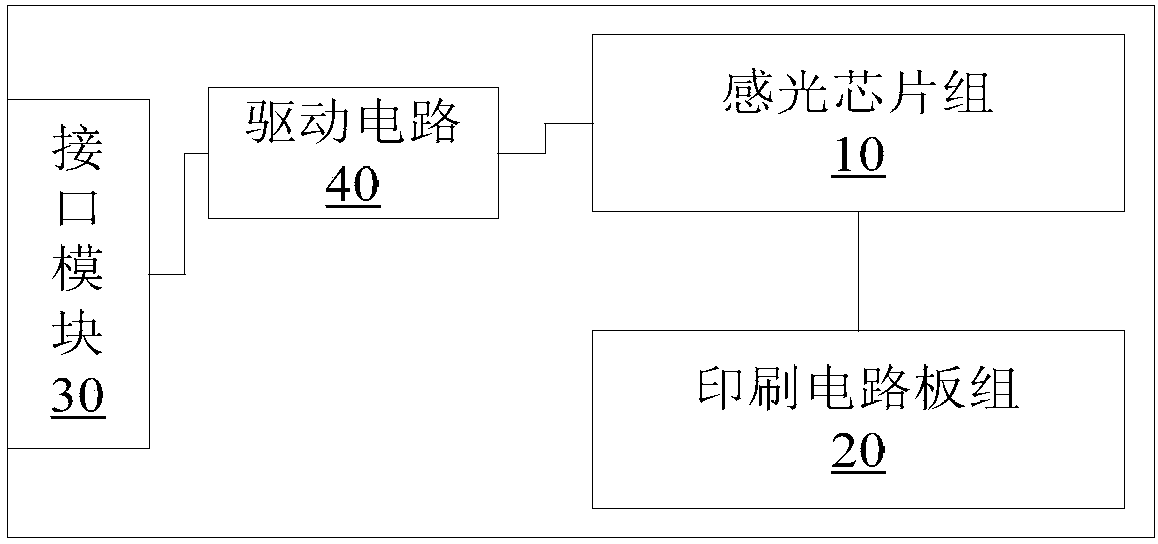
[0042] image 3 is a schematic diagram of an optional image sensor according to an embodiment of the present invention, such as image 3 As shown, the image sensor includes a photosensitive chip set 10, a printed circuit board set 20, an interface module 30 and a drive circuit 40, wherein the photosensitive chip set 10 includes a plurality of photosensitive chips connected in sequence along a preset direction, and each photosensitive chip is used for Convert the light sensed by itself into an electrical signal. In the case of a contact image sensor CIS, each photosensitive chip is used to sense the light reflected by the original, and convert the light reflected by the original sensed by itself into electric signal. The printed circuit board group 20 includes a plurality of printed circuit boards sequentially connected along a predetermined direction, each printed circuit board is connected to at least one photosensitive chip, and each printed circuit board is used to receive...

Embodiment 2

[0051] An image sensor such as Figure 8 As shown, the image sensor includes a light source 1 , a lens 2 , a photosensitive chip 3 , a printed circuit board 4 b , a frame 5 , a base 6 , metal wires 7 and an interface module 9 . The light emitted by the light source 1 is reflected by the original, and is collected by the lens 2 on the photosensitive chip 3 for photoelectric conversion. The electrical signal converted by the photosensitive chip 3 passes through the metal wire 7 and is transmitted to the outside through the interface 9 on the printed circuit board 4b. The base 6 is used to mount the printed circuit board 4 b, and the frame 5 is used to mount the light source 1 and the lens 2 .

[0052] The top view of the abutment 6 is as follows Figure 4 As shown, the right view is as Figure 5 As shown, the bottom view is as Image 6 As shown, a plurality of spliced ​​printed circuit boards 4b and a non-wiring circuit board 4a are mounted on the base 6, and a plurality of p...

Embodiment 3

[0060] An image sensor such as Figure 12 As shown, the image sensor includes a light source 1 , a lens 2 , a photosensitive chip 3 , a printed circuit board 4 b , a frame 5 , a base 6 , metal wires 7 and an interface module 9 . The light emitted by the light source 1 is reflected by the original, and is collected by the lens 2 on the photosensitive chip 3 for photoelectric conversion. The electrical signal converted by the photosensitive chip 3 passes through the metal wire 7 and is transmitted to the outside through the interface 9 on the printed circuit board 4b. The base 6 is used to mount the printed circuit board 4 b, and the frame 5 is used to mount the light source 1 and the lens 2 .

[0061] The top view of the abutment 6 is as follows Figure 13 As shown, the right view is as Figure 14 As shown, the bottom view is as Image 6As shown, a plurality of spliced ​​printed circuit boards 4 b are mounted on the base 6 , and a plurality of photosensitive chips 3 are spli...


PUM


Abstract

The invention discloses an image sensor. The image sensor comprises a light-sensitive chip group comprising a plurality of light-sensitive chips connected in sequence along a preset direction, whereineach light-sensitive chip is used for converting sensed light into an electrical signal; a printed circuit board group comprising a plurality of printed circuit boards connected in sequence along a preset direction, wherein each printed circuit board is connected with at least one light-sensitive chip, and is used for receiving the electrical signal converted by the correspondingly connected light-sensitive chip; an interface module used for executing communication between the image sensor and external equipment; and a driving circuit arranged between the light-sensitive chip group and the interface module, and used for driving the electrical signal transmitted between the image sensor and the external equipment. According to the image sensor provided by the invention, the technical problem that in the prior art, the circuit boards are lengthened and spliced in a large CIS, and thus the signal is attenuated and distorted is solved.

Description

technical field [0001] The present invention relates to the field of sensors, in particular to an image sensor. Background technique [0002] The contact image sensor (CIS for short) is an image sensor that uses multiple circuit boards spliced ​​together to realize large-format image scanning. The contact image sensor (CIS for short) is used to scan the original image, mainly used in fax Machines, scanners, multi-functional all-in-one machines, automatic teller machines, sorting machines, marking machines and other equipment, the scanning width of the contact image sensor used in the above equipment is mostly 183mm ~ 216mm, and the longest scanning width can reach A3 length . With the development of technology, contact image sensors are gradually applied to online inspection, machine vision and other fields, used to scan some textiles, large maps, etc. For some special purposes, the image sensor may require a scanning width of more than one meter. However, since current ci...

Claims


Application Information

Patent Timeline
Patent Type & Authority Applications(China)
IPC IPC(8): H04N1/028H04N1/024
CPCH04N1/024H04N1/028
Inventor 戚务昌王萍咸杰王家重
Owner WEIHAI HUALING OPTO ELECTRONICS CO LTD
Learn More