Semiconductor mid-infrared and visible light dual-wavelength transmission type interference test device

A test device, semiconductor technology, applied in the direction of measurement device, optical device, optical instrument test, etc., can solve the problem of test range limitation

Pending Publication Date: 2018-06-08
赵智亮 +1
View PDF0 Cites 6 Cited by
  • Summary
  • Abstract
  • Description
  • Claims
  • Application Information

AI Technical Summary

Problems solved by technology

Through the dual-band common optical path test, the device realizes the high-precision alignment test of optical components from the visible light band to the mid-infrared band, and solves the problems of the common optical path alignment and test range limitation of the mid-infrared interferometer test.

Method used


Image

  • Semiconductor mid-infrared and visible light dual-wavelength transmission type interference test device

Examples


Embodiment Construction

[0020] The present invention will be described in detail below in conjunction with the accompanying drawings, but the protection scope of the present invention should not be limited thereto.

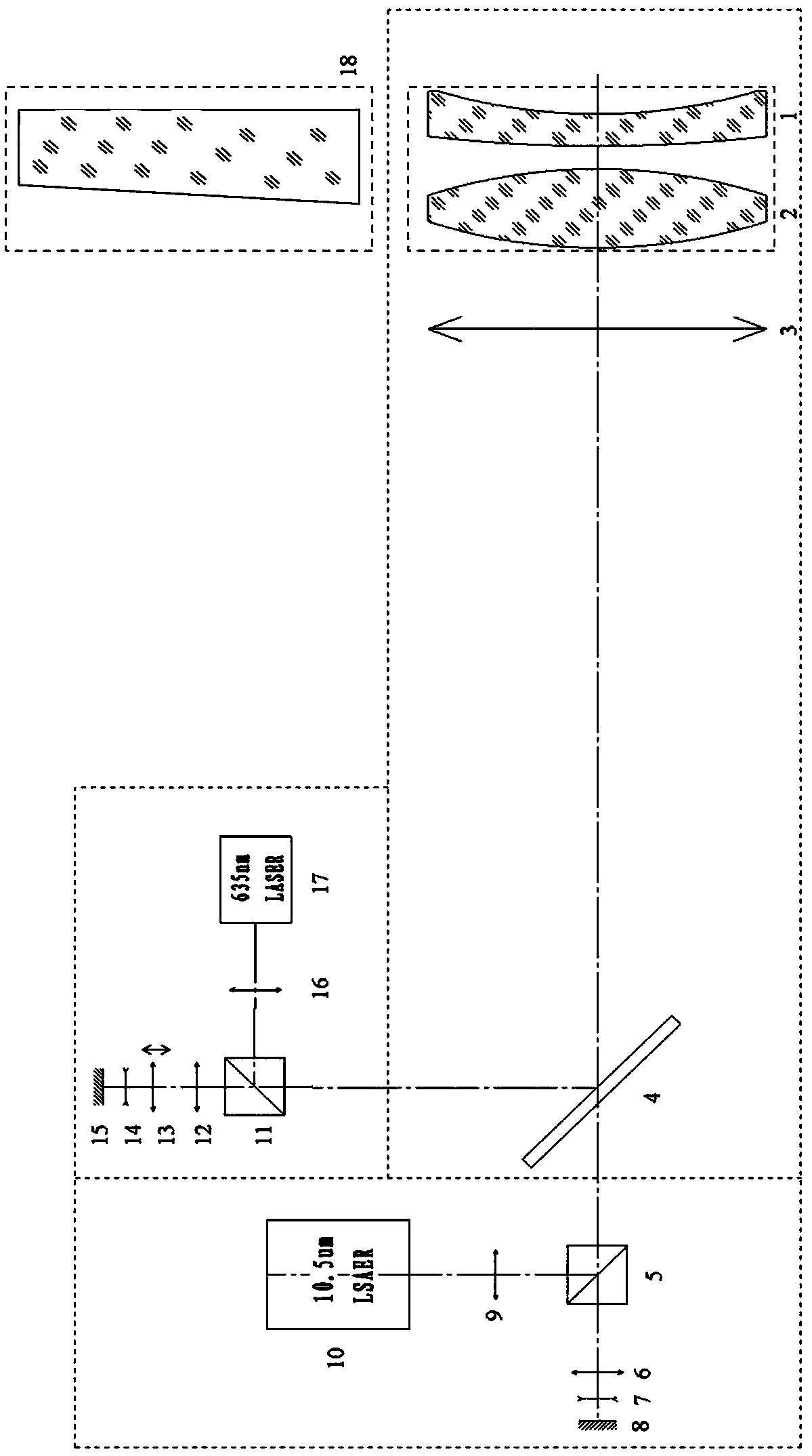
[0021] figure 1 It is the optical path diagram of the semiconductor mid-infrared and visible light dual-wavelength transmission interference test device of the present invention. It can be seen from the figure that the semiconductor mid-infrared and visible light dual-wavelength transmission interference test device of the present invention includes a dual-band common optical path collimation output module and a 10.5 μm semiconductor infrared light Interference imaging module and 635nm semiconductor visible light interference imaging test alignment module:

[0022] The dual-band common optical path collimation output module includes a 635nm semiconductor visible light source 17 and a 10.5 μm semiconductor infrared light source 10. Along the output beam direction of the 10.5 μm semiconduc...


PUM

PropertyMeasurementUnit
transmittivityaaaaaaaaaa
reflectanceaaaaaaaaaa
transmittivityaaaaaaaaaa

Abstract

A semiconductor mid-infrared and visible light dual-wavelength transmission type interference test device used for detecting mid-infrared optical components, materials and optical systems comprises adual-band common-path collimation output module, a 10.5-micron semiconductor infrared light interference imaging module and a 635nm semiconductor visible light interference imaging test alignment module. With the device adopted, high-resolution interference test with mid-infrared test precision PV value higher than 0.05lambda, RMS higher than 0.01lambda and system repeatability higher than 0.001lambda can be realized.

Description

technical field [0001] The invention relates to a mid-infrared and visible light dual-wavelength Fizeau transmission interference test device, which mainly uses a mid-infrared and visible light dual-wavelength semiconductor light source for interference testing, and can be used for testing the surface shape accuracy of mid-infrared optical elements, physical properties of materials and optical systems. Comprehensive characteristic parameters. Background technique [0002] At present, mid-infrared optical systems have broad application prospects in the fields of military, aerospace, energy, communications, remote sensing, etc., which has led to a growing demand for the detection of optical components and materials used in mid-infrared optical systems. Workers pay close attention to the testing of optical products and optical systems in the mid-infrared application band, and have launched a series of related research. Since the end of the 1960s, scientific researchers have st...

Claims


Application Information

Patent Timeline
Patent Type & Authority Applications(China)
IPC IPC(8): G01B11/24G01M11/00G01N21/84
CPCG01B11/2441G01M11/00G01N21/84
Inventor 赵智亮陈利华赵子嘉葛瑞红廖伟李季根刘敏
Owner 赵智亮
Why Eureka
Try Eureka