Ridge waveguide and two-D photonic crystal combined silicon-base Raman laser structure

A two-dimensional photonic crystal and Raman laser technology, applied in the field of silicon-based Raman laser structure, can solve the problems of high end-face flatness requirements, unfavorable integration, etc., achieve high quality factor, reduce complexity, and be beneficial to laser lasing effect

Inactive Publication Date: 2006-12-13
INST OF SEMICONDUCTORS - CHINESE ACAD OF SCI
View PDF0 Cites 8 Cited by
  • Summary
  • Abstract
  • Description
  • Claims
  • Application Information

AI Technical Summary

Problems solved by technology

This structure has its disadvantages. It needs to be coated with multi-layer reflective film on the end face, which has high requirements on the flatness of the end face. Because the film is coated on both end faces, this structure is not conducive to the integration with other devices.

Method used


Image

  • Ridge waveguide and two-D photonic crystal combined silicon-base Raman laser structure
  • Ridge waveguide and two-D photonic crystal combined silicon-base Raman laser structure
  • Ridge waveguide and two-D photonic crystal combined silicon-base Raman laser structure

Examples


Embodiment Construction

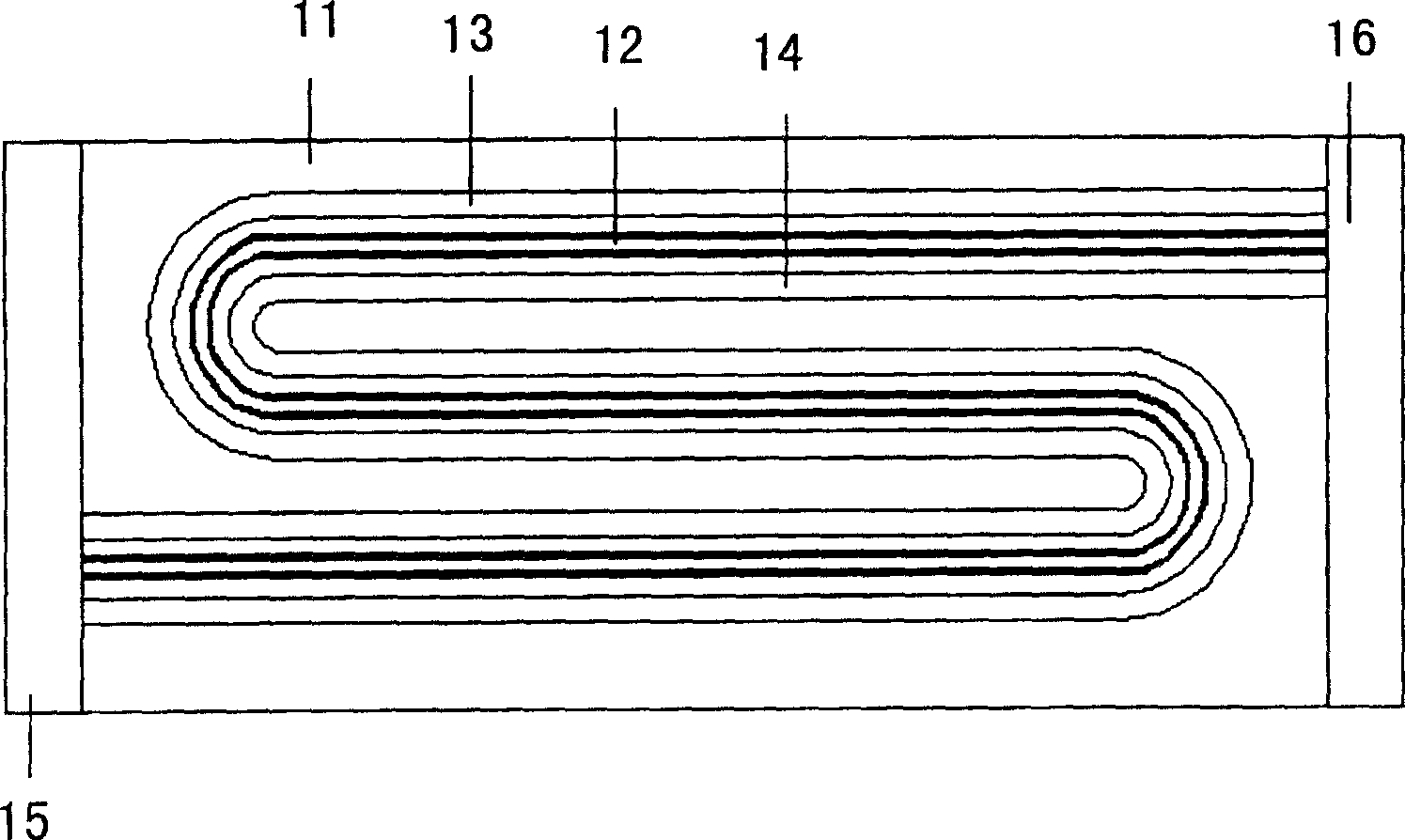
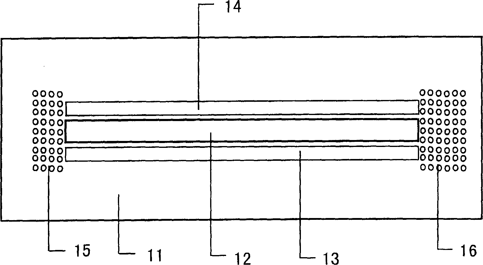
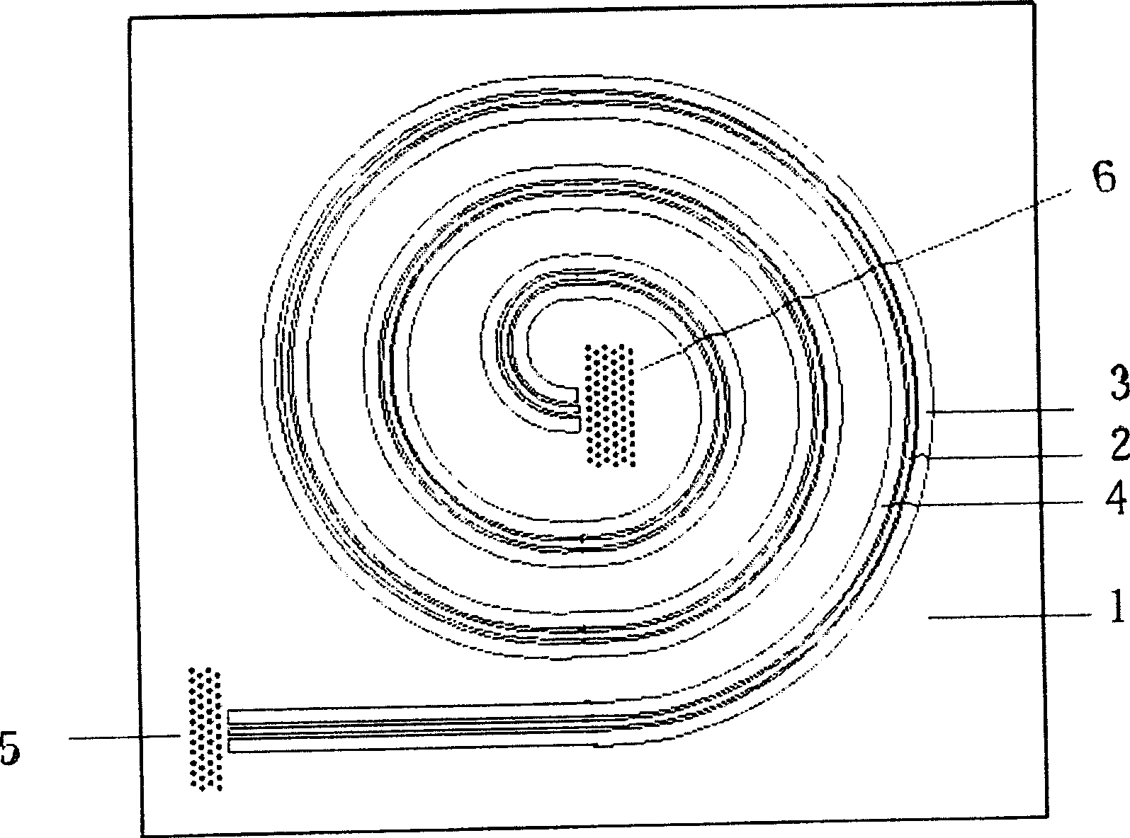
[0031] see image 3 As shown, a silicon-based Raman laser structure combining a ridge waveguide and a two-dimensional photonic crystal of the present invention includes:

[0032] An SOI material 1; the SOI material 1 includes: a silicon substrate 9; a silicon dioxide insulating layer 8, the silicon dioxide insulating layer 8 is made on the silicon substrate 9; a top layer of silicon 7, the top layer of silicon 7 is made On the silicon dioxide insulating layer 8; the thickness of the silicon dioxide insulating layer 8 is 1-2 microns, and the thickness of the top silicon layer 7 is 1-5 microns;

[0033] A ridge waveguide 2, the ridge waveguide 2 is made on the SOI material 1, the ridge waveguide 2 is a single-mode waveguide satisfying the single-mode condition of the ridge waveguide, the cross section of the waveguide is trapezoidal or rectangular, and the overall shape is spiral or rectangular or zigzag or other shape;

[0034] A P-type silicon 3, the P-type silicon 3 is fabr...


PUM


Abstract

The invention discloses a silicon-based Longman laser structure with combination of ridge waveguide and two-dimension photon crystal, which comprises the following parts: SOI material, ridge waveguide on the SOI material, P-typed silicon on one side of ridge waveguide, N-typed silicon on one side of ridge waveguide, photon crystal rear reflecting mirror on the rear end of ridge waveguide on the SOI material, photon crystal front reflecting mirror on the input end of ridge waveguide on the SOI material, wherein the photon crystal front end and rear reflecting mirrors and ridge waveguide form laser resonant cavity; the photon crystal reflects all light.

Description

technical field [0001] The invention is a silicon-based Raman laser structure combining a ridge waveguide and a two-dimensional photonic crystal. The two-dimensional photonic crystal is used as the end mirror of the resonant cavity, and the single-mode ridge waveguide is used as the resonant cavity. Background technique [0002] On February 17, 2005, the US "Nature" magazine reported the world's first continuous wave silicon-based Raman laser (Haisheng Rong, Richard Jones, Ansheng Liu, Oded Cohen, Dani Hak Alexander Fang, Mario Paniccia, A continuous- wave Raman siliconlaser, NATURE, 433 (2005) 725-728), which is an important milestone in the research of silicon-based optoelectronic devices and their integration. [0003] At present, the main bottleneck in the development of semiconductor chips used to process data lies in the computing speed of the chip. Part of the reason for this bottleneck is the physical properties of metals: the metal has resistance, which limits the c...

Claims


Application Information

Patent Timeline
Patent Type & Authority Applications(China)
IPC IPC(8): H01S5/22H01S5/10
Inventor 许兴胜王春霞陈弘达
Owner INST OF SEMICONDUCTORS - CHINESE ACAD OF SCI
Why Eureka
Try Eureka