Method for manufacturing transparent flexible multilayer PCB

A production method and transparent technology, applied in printed circuit manufacturing, conductive pattern formation, ink, etc., can solve the problems that hard PCBs are not easy to bend and deform, easy to break, and low transparency, so as to improve production efficiency, simple production method, Ease of transport

Active Publication Date: 2018-06-19
SHENZHEN UNIV
View PDF4 Cites 5 Cited by
  • Summary
  • Abstract
  • Description
  • Claims
  • Application Information

AI Technical Summary

Problems solved by technology

[0004] The main purpose of the present invention is to provide a method for manufacturing a transparent flexible multilayer PCB, which can solve the technical problems in the prior art that the hard PCB is not easily deformed, easily broken, and has low transparency.

Method used


Image

  • Method for manufacturing transparent flexible multilayer PCB
  • Method for manufacturing transparent flexible multilayer PCB
  • Method for manufacturing transparent flexible multilayer PCB

Examples


Embodiment Construction

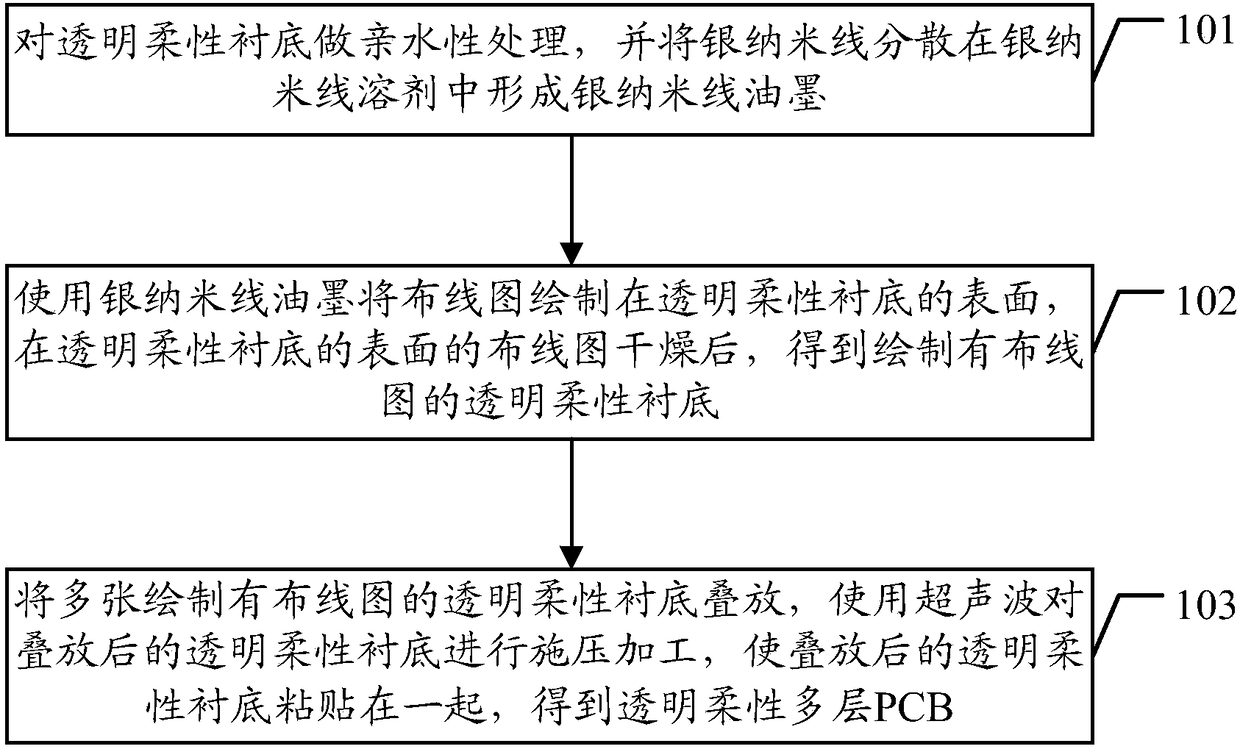
[0027] In order to make the purpose, features and advantages of the present invention more obvious and understandable, the technical solutions in the embodiments of the present invention will be clearly and completely described below in conjunction with the accompanying drawings in the embodiments of the present invention. Obviously, the described The embodiments are only some of the embodiments of the present invention, but not all of them. Based on the embodiments of the present invention, all other embodiments obtained by those skilled in the art without making creative efforts belong to the protection scope of the present invention.

[0028] In the prior art, there are technical problems that the hard PCB is not easy to be bent, deformed, easily broken, and the transparency is not high.

[0029] In order to solve the above technical problems, the present invention proposes a method for manufacturing a transparent flexible multilayer PCB. Since the transparent flexible sub...


PUM

PropertyMeasurementUnit
diameteraaaaaaaaaa
lengthaaaaaaaaaa
transmittivityaaaaaaaaaa

Abstract

The invention discloses a method for manufacturing a transparent flexible multilayer PCB. The method comprises steps of: subjecting a transparent flexible substrate to hydrophilic treatment, dispersing silver nanowires in a silver nanowire solvent to form silver nanowire ink, drawing a wiring pattern on the surface of the transparent flexible substrate by using the silver nanowire ink, drying thewiring pattern, stacking a plurality of transparent flexible substrates on which wiring patterns are drawn, applying pressure to the stacked transparent flexible substrates by using ultrasonic, and pasting the stacked transparent flexible substrates together to obtain the transparent and flexible multilayer PCB. Since the transparent flexible substrate is transparent and flexible, the transparentflexible multilayer PCB is transparent, less likely to deform or fracture. Since the silver nanowires have low surface resistance, the PCB has low square resistance. The manufacturing method is simple, can easily use a roll-to-roll industrialized continuous production method, improves the production efficiency and facilitates transportation.

Description

technical field [0001] The invention relates to the field of nanomaterial composite films, in particular to a method for manufacturing a transparent flexible multilayer printed circuit board (Printed Circuit Board, PCB). Background technique [0002] Usually, printed circuits, printed components, or a combination of the two are called printed circuits on an insulating substrate according to a predetermined design, and electrical circuits between components are provided on an insulating substrate. The connected conductive pattern is called a printed circuit. In this way, the finished board of printed circuit or printed circuit is called printed circuit board. [0003] Most of the PCBs currently on the market are rigid PCBs. Obviously, the disadvantage of rigid PCB is that it is not easy to bend, deform and break easily, and its transparency is not high. Contents of the invention [0004] The main purpose of the present invention is to provide a method for manufacturing a...

Claims


Application Information

Patent Timeline
Patent Type & Authority Applications(China)
IPC IPC(8): H05K3/12H05K1/09C09D11/52
CPCC09D11/52H05K1/097H05K3/12H05K2203/0285H05K2203/0502
Inventor 向雄志彭湃黄东炎邱克垚张国良
Owner SHENZHEN UNIV
Why Eureka
Try Eureka