

An MEMS piezoelectric sensor and a manufacturing method thereof
A kind of piezoelectric sensor, technology of making method
- Summary
- Abstract
- Description
- Claims
- Application Information
AI Technical Summary
Problems solved by technology
Method used
Image

Examples
Embodiment Construction
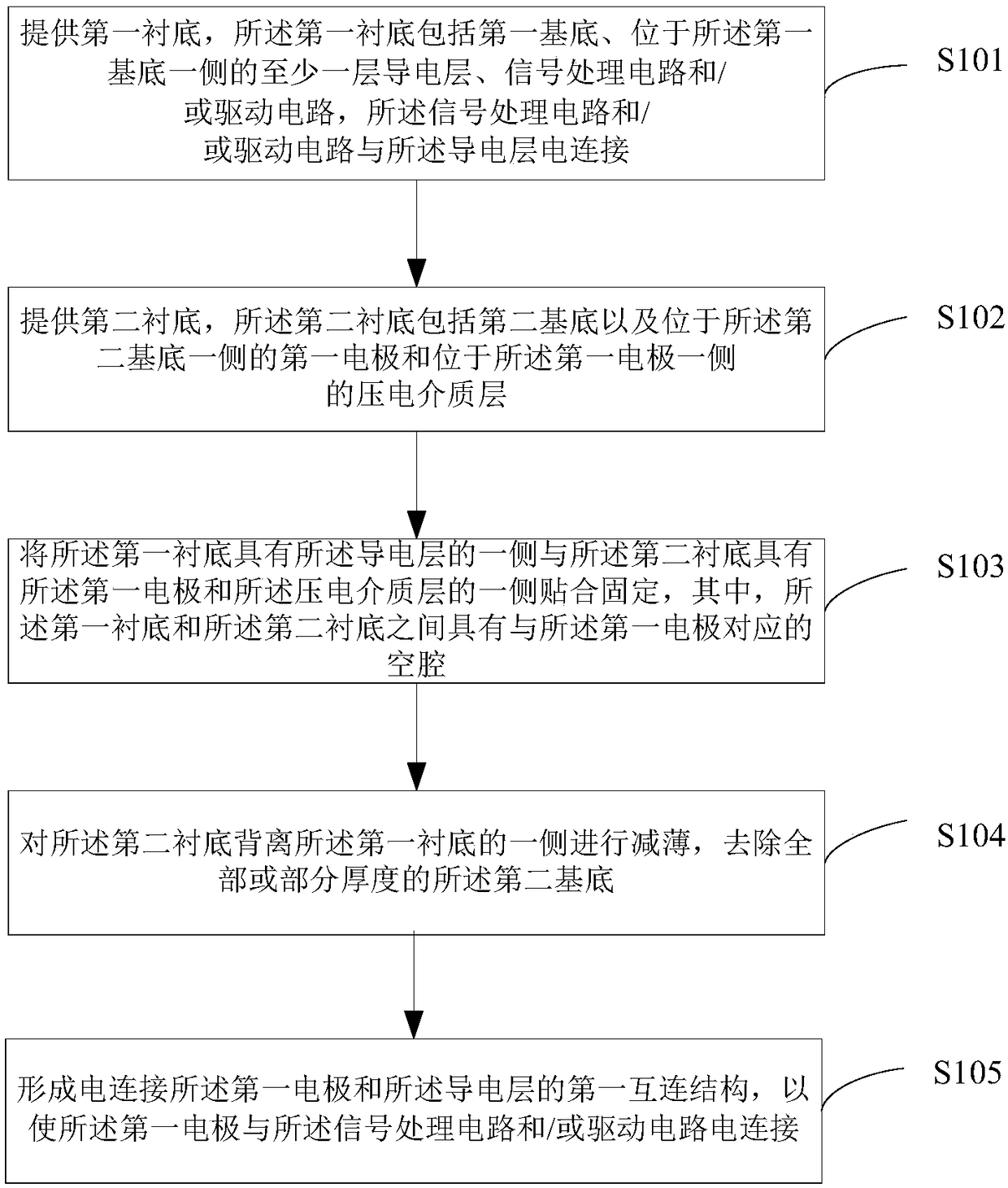
[0112] The following will clearly and completely describe the technical solutions in the embodiments of the present invention with reference to the accompanying drawings in the embodiments of the present invention. Obviously, the described embodiments are only some, not all, embodiments of the present invention. Based on the embodiments of the present invention, all other embodiments obtained by persons of ordinary skill in the art without making creative efforts belong to the protection scope of the present invention.
[0113] One embodiment of the present invention provides a kind of fabrication method of MEMS piezoelectric sensor, such as figure 1 shown, including:
[0114] S101: Provide a first substrate, the first substrate includes a first substrate, at least one conductive layer on one side of the first substrate, a signal processing circuit and / or a driving circuit, the signal processing circuit and / or or the driving circuit is electrically connected to the conductive...
PUM
 Abstract
Description
Claims
Application Information