Array substrate and preparation method thereof, and display panel

A technology for array substrates and display panels, applied to semiconductor devices, electrical components, circuits, etc., can solve the problems of reducing the connection reliability between pixel electrodes and drain electrodes, reducing the transmittance of display panels, and increasing the difficulty of preparing via holes, etc., to achieve Good application prospects, little impact on performance, and easy implementation

Active Publication Date: 2018-06-29
BOE TECH GRP CO LTD +1
View PDF18 Cites 9 Cited by
  • Summary
  • Abstract
  • Description
  • Claims
  • Application Information

AI Technical Summary

Problems solved by technology

But these solutions can seriously affect the quality of the display panel
For example, the solution of increasing the distance between the pixel electrode and the data line will lead to a decrease in aperture ratio, which not only reduces the transmittance of the display panel, but also restricts the improvement of resolution
As another example, the solution of increasing the thickness of the insulating layer between the pixel electrode and the data line will increase the difficulty of preparing the via hole, reduce the reliability of the connection between the pixel electrode and the drain electrode, and cause the risk of disconnection, and also reduce the display to a certain extent. panel transmittance

Method used


Image

  • Array substrate and preparation method thereof, and display panel
  • Array substrate and preparation method thereof, and display panel
  • Array substrate and preparation method thereof, and display panel

Examples


no. 1 example

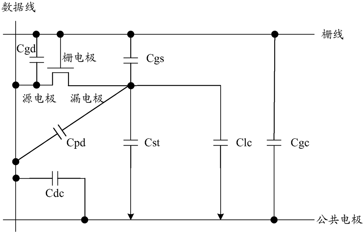
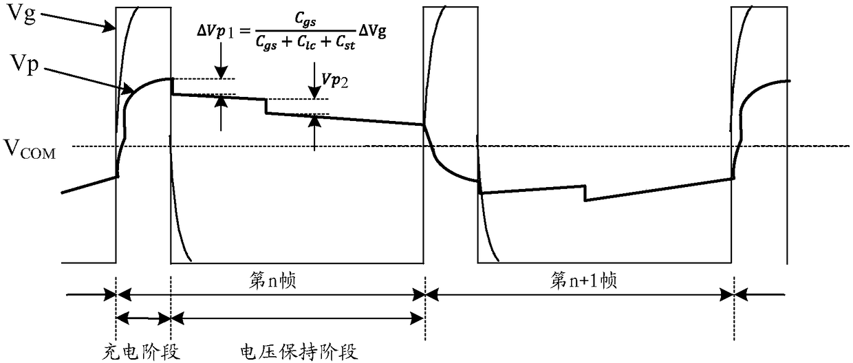
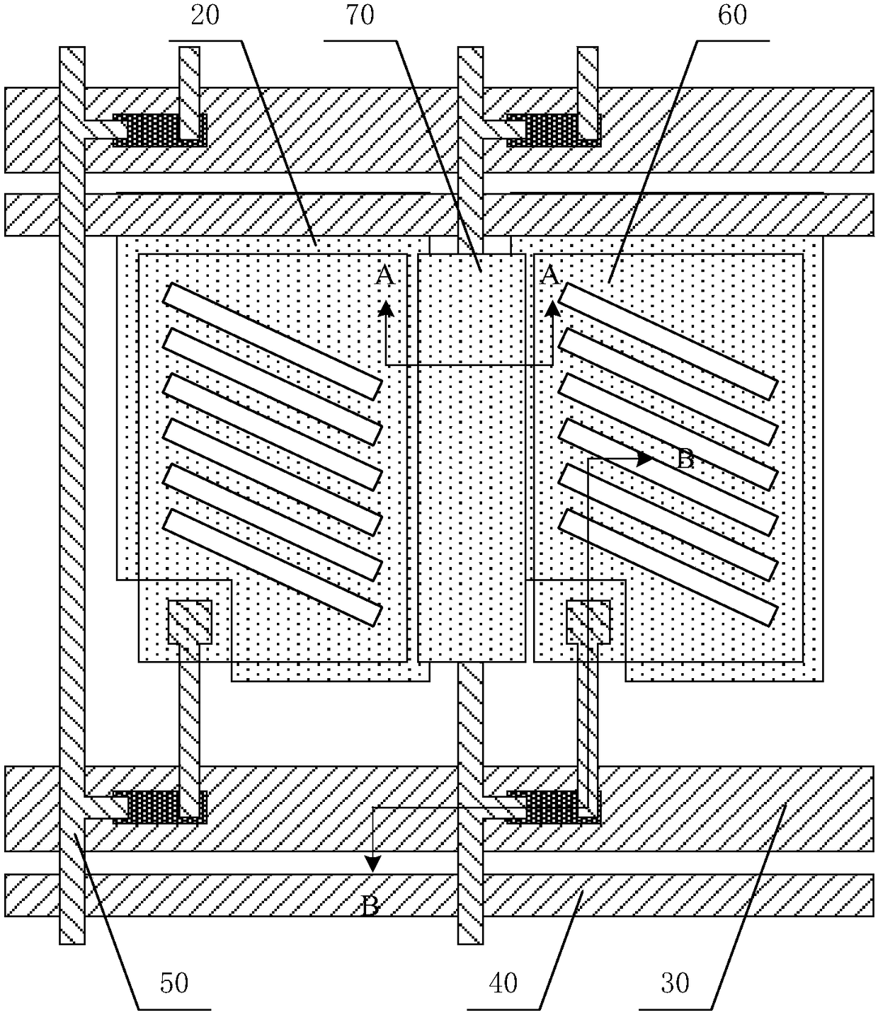
[0059] Figure 3A is a schematic structural diagram of the first embodiment of the array substrate of the present invention, Figure 3B for Figure 3A The cross-sectional view of A-A in the middle. The main structure of the array substrate in this embodiment includes a base, a plurality of gate lines and a plurality of data lines arranged on the base, the plurality of gate lines and data lines intersect each other to define a plurality of pixel areas arranged in an array, and each pixel area is set There are thin film transistors, common electrodes, pixel electrodes and shield electrodes. Such as Figure 3A and Figure 3B As shown, the array substrate of this embodiment includes a substrate 10, a common electrode 20 disposed on the substrate 10, a gate line 30, a common electrode line 40, a data line 50, a pixel electrode 60 and a shielding electrode 70, and the shielding electrode 70 covers the data line 50, and connected to the common electrode 20 through the via holes ...

no. 2 example

[0082] Figure 10A is a schematic structural diagram of the second embodiment of the array substrate of the present invention, Figure 10B for Figure 10A The cross-sectional view of A-A in the middle. The main structure of the array substrate in this embodiment includes a base, a plurality of gate lines and a plurality of data lines arranged on the base, the plurality of gate lines and data lines intersect each other to define a plurality of pixel areas arranged in an array, and each pixel area is set There are thin film transistors, common electrodes, pixel electrodes and shield electrodes. Such as Figure 10A and Figure 10B As shown, the array substrate of this embodiment includes a substrate 10, the gate lines 30, the common electrode lines 40, the pixel electrodes 60 and the shielding electrodes 70 are arranged on the substrate 10, and the gate insulating layer 12 covers the gate lines 30, the common electrode lines 40, and the pixel electrodes. electrode 60 and shi...

no. 3 example

[0102] Figure 17 is a schematic structural diagram of the third embodiment of the array substrate of the present invention, which is Figure 10A The cross-sectional view of A-A in the middle. This embodiment is a structural modification of the second embodiment, and the main structure of the array substrate is basically the same as that of the second embodiment. In the second embodiment, the common electrode is an integral structure, that is, the common electrode above the data line and the common electrode above the pixel electrode are of an integrated structure. The difference from the second embodiment is that the common electrode in this embodiment is a separate structure, that is, the common electrode above the data line and the common electrode above the pixel electrode are separate structures. Such as Figure 17 As shown, the first common electrode 20a is located above the pixel electrode 60 and is a slit electrode with a certain inclination angle, the second common...


PUM


Abstract

The embodiment of the invention provides an array substrate and a preparation method thereof, and a display panel. The array substrate comprises a first electrode, a first insulation layer, a data line, a second insulation layer and a second electrode which are arranged on the substrate in order; two sides of the data line are provided with isolation via holes, and the second electrode is connected with the first electrode through the isolation via holes. A shielding electrode connected with a common electrode is arranged and shielding walls are formed at two sides of the data line to shield the capacitance coupling effect between the pixel electrode and the data line and eliminate the pixel voltage abrupt change caused by the coupling capacitance between the data line and the pixel electrode to the most extent. The array substrate and the preparation method thereof, and the display panel are simple in preparation process, low in production cost and convenient to implement.

Description

technical field [0001] The invention relates to the field of display technology, in particular to an array substrate, a preparation method thereof, and a display panel. Background technique [0002] Thin Film Transistor Liquid Crystal Display (TFT-LCD) is the current mainstream flat panel display panel, which has the advantages of light weight, small size, low power consumption, no radiation, and high display resolution. The main structure of TFT-LCD includes an array substrate and a color filter substrate in the box. On the array substrate, gate lines, data lines, and thin-film transistors and pixel electrodes arranged in a matrix are formed. Control signals applied on the gate lines make the data lines The signal voltage of the signal is transmitted to the pixel electrode, and the voltage is provided to the common electrode at the same time, so that the common electrode and the pixel electrode form an electric field, and the arrangement direction of the liquid crystal mole...

Claims


Application Information

Patent Timeline
IPC IPC(8): H01L27/32
CPCH10K59/122H10K59/123H10K59/121H10K59/131
Inventor 蒋学兵高吉磊
Owner BOE TECH GRP CO LTD
Why Eureka
Try Eureka