Device package structure and method for stress release in packaging process

A technology for stress release and device packaging, which is applied in the manufacture of electrical solid devices, semiconductor devices, semiconductor/solid devices, etc., can solve problems such as prone to warping, impossibility of follow-up processes, and affecting the quality and performance of packaged products, so as to improve Quality and performance, suitable for mass production

Inactive Publication Date: 2018-07-06
NINGBO SEMICON INT CORP
View PDF9 Cites 12 Cited by
  • Summary
  • Abstract
  • Description
  • Claims
  • Application Information

AI Technical Summary

Problems solved by technology

However, after the wafer is plastic-encapsulated, it is easy to warp, which may cause the subsequent process to fail or require special treatment and adjustment in the subsequent process, which will affect the quality and performance of the packaged product.

Method used


Image

  • Device package structure and method for stress release in packaging process
  • Device package structure and method for stress release in packaging process
  • Device package structure and method for stress release in packaging process

Examples


Embodiment Construction

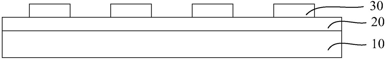
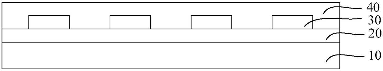
[0034] Figure 1a~1c It is a structural schematic diagram of each step of a device packaging method. Such as Figure 1a ~ Figure 1c As shown, the device packaging method includes the following steps: first: provide a carrier part 10, form an adhesive layer 20 on the carrier part 10, and then fix a plurality of units to be packaged 30 on the adhesive layer 20 at intervals . Secondly, a plastic sealing layer 40 is formed on the adhesive layer 20, and the plastic sealing layer 40 covers the adhesive layer 20 and the unit 30 to be packaged. Finally, the adhesive layer 20 loses its viscosity by ultraviolet light irradiation, heating or other methods, and the carrying part 10 and the adhesive layer 20 are removed, finally forming a device packaging structure. However, due to the thermal expansion and contraction characteristics of each material in the device packaging structure, volume changes will occur under the action of temperature, resulting in strain; when the strain of the ...


PUM


Abstract

The present invention provides a device package structure and a method for stress release in a packaging process. The method includes the following steps that: a carrying component is provided, a plurality of units to be packaged are fixed onto the carrying component at intervals; a plastic package layer is formed on the carrying component, wherein the plastic package layer covers the carrying component and the units to be packaged; and a plurality of stress release openings are formed in the plastic package layer. Since the stress release openings are capable of releasing stress inside the plastic package layer, so that the warpage of the units to be packaged which have been subjected to plastic package can be decreased, and therefore, subsequent process manufacture can be facilitated. The method is suitable for mass production and can improve the quality and performance of the device package structure.

Description

technical field [0001] The invention relates to the technical field of semiconductors, in particular to a device packaging structure and a method for releasing stress during the packaging process. Background technique [0002] Wafer Level Packaging (WLP) technology is a technology that performs packaging and testing on the entire wafer and then cuts it to obtain a single finished chip. Require. The size of the chip packaged by wafer-level packaging technology has reached a high degree of miniaturization, and the cost of the chip will be significantly reduced with the reduction of the chip size and the increase of the wafer size. It is a hot spot in the current packaging field and a future development trend. [0003] When performing wafer packaging, especially fan-out wafer packaging (FOWLP), the chip is placed on the carrier part with the adhesive layer formed, and then the carrier part is plastic-sealed to form a plastic package, and then irradiated or heated by ultraviole...

Claims


Application Information

Patent Timeline
Patent Type & Authority Applications(China)
IPC IPC(8): H01L21/56H01L23/31H01L23/00
CPCH01L21/56H01L23/3171H01L23/3185H01L23/562H01L2224/96
Inventor 杨天伦
Owner NINGBO SEMICON INT CORP
Why Eureka
Try Eureka