Supercharge Your Innovation With Domain-Expert AI Agents!

Semiconductor device

A technology of semiconductors and devices, which is applied in the field of semiconductor devices to achieve the effect of ensuring margins

Active Publication Date: 2018-07-20
SK HYNIX INC
View PDF6 Cites 3 Cited by
  • Summary
  • Abstract
  • Description
  • Claims
  • Application Information

AI Technical Summary

Problems solved by technology

With increased input / output speed of data, the probability of errors during the data transfer process increases

Method used


Image

  • Semiconductor device
  • Semiconductor device
  • Semiconductor device

Examples


Embodiment Construction

[0022] Hereinafter, a semiconductor device will be described below with reference to the accompanying drawings through various examples of embodiments.

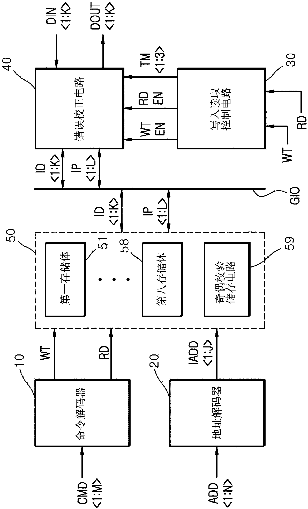
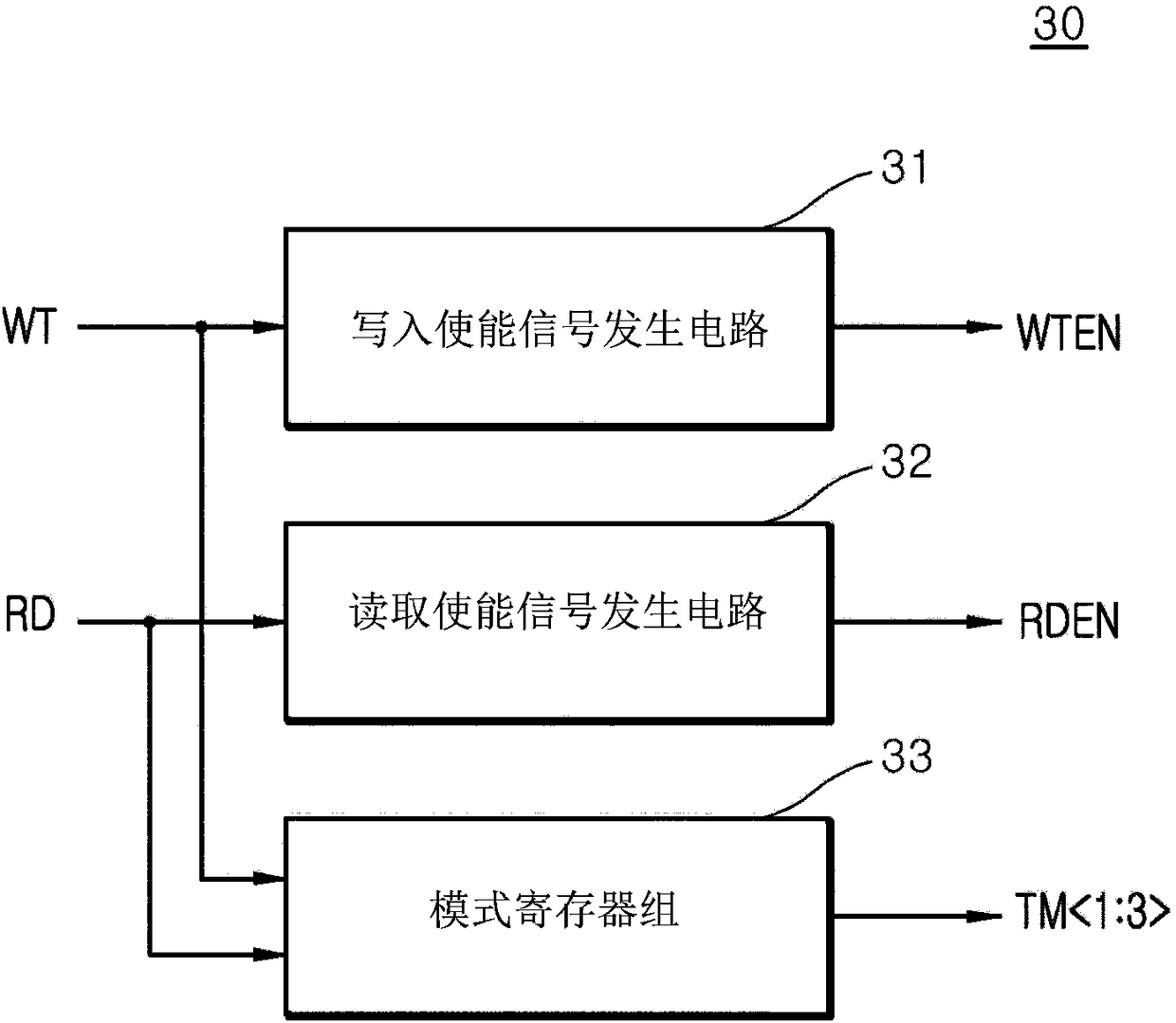
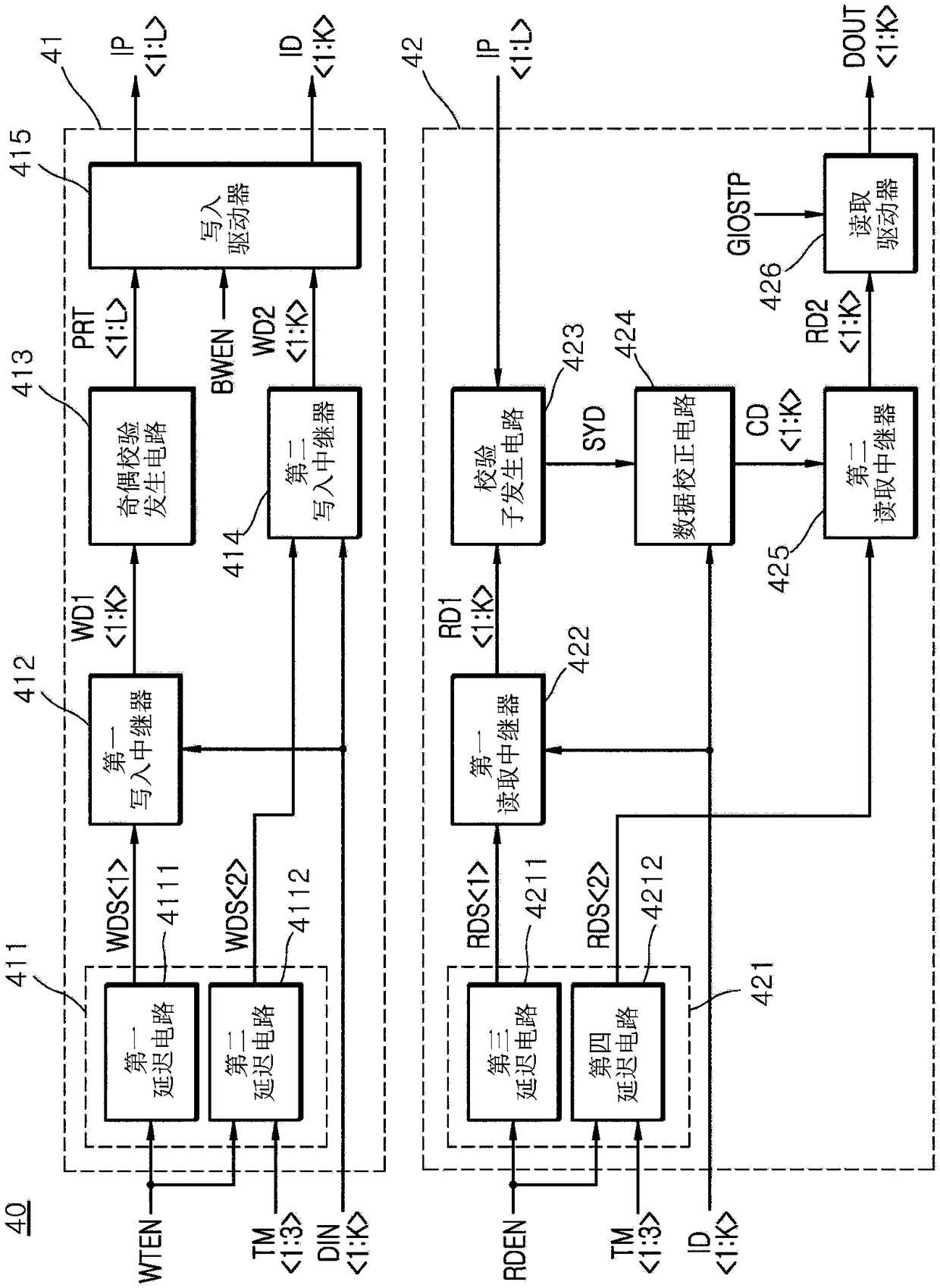
[0023] Such as figure 1 As shown in , a semiconductor device according to one embodiment may include a command decoder 10 , an address decoder 20 , a write read control circuit 30 , an error correction circuit 40 and a memory circuit 50 .

[0024] The command decoder 10 can decode the command CMD, and generate a write command WT and a read command RD. The command CMD may be set as a signal input from a controller or test equipment that controls a semiconductor device. The command CMD may be transmitted via a line transmitting at least one of address, command, and data. The bit number M of the command CMD may be set as a natural number, and is set to various bit numbers according to embodiments. The write command WT may be set as a command for entering a write operation. A read command RD may be set as a command for enteri...


PUM


Abstract

A semiconductor device includes a write read control circuit for outputting a write enable signal which is enabled in response to a write command, and a test mode signal; and an error correction circuit suitable for performing a calculation operation of determining an error information of input data in response to the write enable signal and then outputting an internal parity signal including theerror information, and outputting internal data by delaying the input data in response to the write enable signal.

Description

[0001] Cross References to Related Applications [0002] This application claims priority from Korean Patent Application No. 10-2017-0004431 filed with the Korean Intellectual Property Office on January 11, 2017, the entire contents of which are hereby incorporated by reference in their entirety. technical field [0003] Embodiments of the present disclosure relate to a semiconductor device that performs an error correction operation on data. Background technique [0004] Recently, in order to increase the operating speed of semiconductor devices, DDR2 or DDR3 signaling in which 4-bit or 8-bit data is input / output per clock cycle is used. As the input / output speed of data increases, the probability of errors occurring during the data transmission process increases. Therefore, separate devices and methods for ensuring the reliability of data transmission are additionally required. [0005] Disclosed is a method for generating error codes capable of checking errors each time...

Claims


Application Information

Patent Timeline
Patent Type & Authority Applications(China)
IPC IPC(8): G11C13/00
CPCG11C13/0069G11C29/14G11C29/42G11C29/46G11C2207/229G06F11/1048G11C29/52G11C11/4096G11C11/4076G11C7/22G11C7/1078G11C7/1051G11C8/12G06F11/1068
Inventor 李在仁金溶美
Owner SK HYNIX INC
Features
  • R&D
  • Intellectual Property
  • Life Sciences
  • Materials
  • Tech Scout
  • Unparalleled Data Quality
  • Higher Quality Content
  • 60% Fewer Hallucinations
Learn More