OLED display panel and OLED display device

A display panel and encapsulation layer technology, which is applied in the manufacture of electrical components, electrical solid devices, semiconductor/solid device, etc., can solve the problems of insufficient brightness of transparent display, small aperture ratio of display panel, etc., and achieve the goal of increasing brightness and aperture ratio Effect

Active Publication Date: 2018-07-20
WUHAN CHINA STAR OPTOELECTRONICS SEMICON DISPLAY TECH CO LTD
View PDF5 Cites 0 Cited by
  • Summary
  • Abstract
  • Description
  • Claims
  • Application Information

AI Technical Summary

Problems solved by technology

However, the display panel formed by the aforementioned OLED devices not only has a small aperture ratio, but also has insufficient brightness for transparent display.

Method used


Image

  • OLED display panel and OLED display device
  • OLED display panel and OLED display device
  • OLED display panel and OLED display device

Examples


no. 1 approach

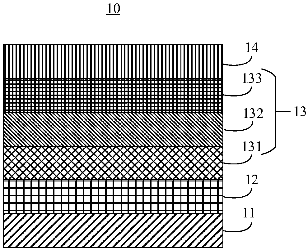
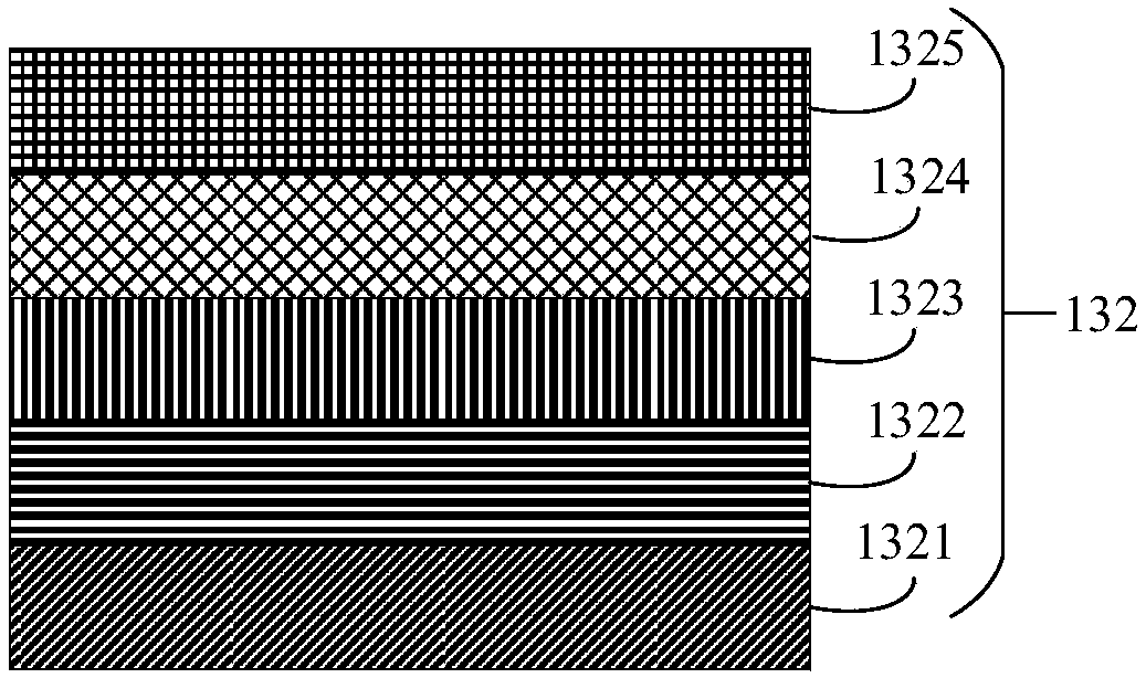
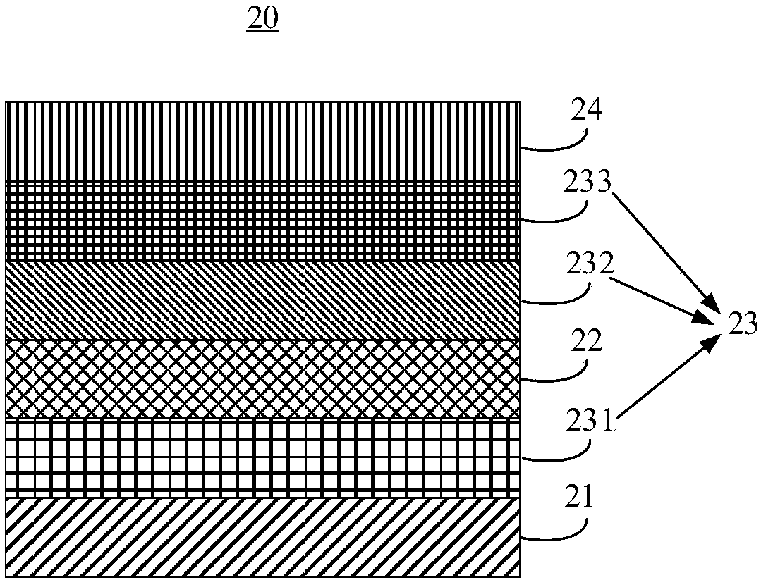
[0047] Different from the first embodiment, the location of the antireflection layer 22 in this embodiment is different. In this embodiment, the antireflection layer 22 is arranged between the anode layer 231 and the hole injection layer 2321, wherein the antireflection layer 22 The refractive index of the hole injection layer 2321 is lower than that of the hole injection layer 2321. In one embodiment, the refractive index of the hole injection layer 2321 ranges from 1.5 to 1.8, and the refractive index of the antireflection layer 22 ranges from 1.2 to 1.4.

[0048] The manufacturing process of the OLED display panel 20 of this embodiment is basically the same as that of the first embodiment, but it is different from the first embodiment. After 231 is prepared, the antireflection layer 22 is fabricated, and then the hole injection layer 2321, the hole transport layer 2322, the light emitting layer 2323, the electron transport layer 2324, the electron injection layer 2325, the ...


PUM


Abstract

The invention discloses an OLED display panel and an OLED display device. The OLED display panel comprises a device layer, an organic light-emitting layer arranged on the device layer, and an encapsulation layer overlying the organic light-emitting layer. At least one anti-reflection layer is arranged between the device layer and the encapsulation layer. Because of the low refractive index of theanti-reflection layer, the total reflection angle of the light emitted by the organic light-emitting layer can be reduced and thus most of light rays emitted by the organic light-emitting layer are emitted in a same direction, so that the brightness of the transparent display of the display panel is improved while no extra transparent area is added; and the aperture ratio of the display panel is also improved.

Description

technical field [0001] The invention relates to the field of display technology, in particular to an OLED display panel and an OLED display device. Background technique [0002] Organic light emitting diodes (organic light emitting diode, OLED) have many excellent characteristics such as self-illumination, low energy consumption, wide viewing angle, fast response, etc., and the panels made of OLEDs have the characteristics of simple structure and bendability. The industry is of great interest and is considered to be a very promising next-generation display technology. Transparent display is also a major direction of display technology development due to its application prospects in 3D display, vehicle display and other fields. [0003] At present, the pixels where the OLED devices used for transparent display are located are opaque, and a transparent display is realized by leaving a transparent area between pixels. However, the display panel formed by the aforementioned OL...

Claims


Application Information

Patent Timeline
Patent Type & Authority Applications(China)
IPC IPC(8): H01L51/52
CPCH10K50/856
Inventor 巫君杰
Owner WUHAN CHINA STAR OPTOELECTRONICS SEMICON DISPLAY TECH CO LTD
Why Eureka
Try Eureka