A method for testing the interface state of a three-port silicon carbide-based power device

A port silicon carbide and testing method technology, which is applied in the direction of single semiconductor device testing, semiconductor working life testing, instruments, etc., can solve the problem that it is difficult to measure the interface state reliably and accurately

Active Publication Date: 2020-04-10
SOUTHEAST UNIV +1
View PDF6 Cites 0 Cited by
  • Summary
  • Abstract
  • Description
  • Claims
  • Application Information

AI Technical Summary

Problems solved by technology

Because the interface state generated under external stress has the characteristics of non-uniform distribution, it is difficult to reliably and accurately measure the interface state generated by the device under external stress by the traditional capacitance (C-V) method. The invention provides a three Test method for interface state of SiC-based power devices with ports

Method used


Image

  • A method for testing the interface state of a three-port silicon carbide-based power device
  • A method for testing the interface state of a three-port silicon carbide-based power device
  • A method for testing the interface state of a three-port silicon carbide-based power device

Examples


Embodiment Construction

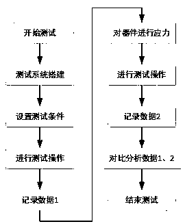
[0029] A method for testing an interface state of a three-port silicon carbide-based power device, comprising the following test steps:

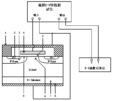
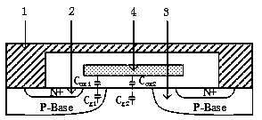
[0030] a) Test system construction: the source 1 of the power device is externally connected to a reverse bias voltage source, the positive pole of the voltage source is connected to the drain 8 of the power device, and the negative pole of the voltage source is connected to the source 1 of the power device, so that the P-type base region 3 and the junction The PN junction of the type field effect region 6 is reverse-biased, and the drain 8 is used as a test current lead-out port to connect an ammeter and the ammeter is connected in series in a circuit composed of the drain 8, the voltage source and the source 1, and the gate 4 is connected with a pulse voltage , the test instrument that the present invention adopts is the Keithley 4200 semiconductor characteristic analyzer of Keithley Company;

[0031] b) Test operation: add a grid pulse vo...


PUM


Abstract

A method for testing the interface state of a three-port silicon carbide-based power device. This method can simply and quickly extract the average interface state density at the interface between the junction field effect region and the gate oxide layer of the three-port silicon carbide-based power device. The frequency and amplitude of the external gate of silicon carbide-based power devices are fixed and the base voltage V 0 Varying pulse voltage or frequency and base voltage V 0 fixed while the amplitude V p The changing pulse voltage, the source is connected to the negative pole of the reverse bias voltage, the drain is connected to the positive pole of the reverse bias voltage, the drain is connected to the ammeter to detect the current, and the ammeter is connected in series in the loop composed of the drain, voltage source, and source, and a The current-voltage curve, the average distribution of the interface state along the junction field effect region can be obtained by calculating the peak current of the current-voltage curve through the formula. At the same time, the junction field effect region and the channel of the device can be judged by comparing the test curves before and after stress. The degradation of the interface of the gate oxide layer under stress.

Description

technical field [0001] The invention belongs to the field of reliability of power semiconductor devices, and in particular relates to an interface state testing method of a three-port silicon carbide-based power device. Background technique [0002] With the improvement of the performance and reliability requirements of power devices in the automotive industry and portable electronic systems, three-port SiC-based power devices stand out because of their high input impedance, low drive power, high switching speed, and good thermal stability. As a switching device, SiC-based power devices need to be turned on and off frequently. During the switching process, the current and voltage vary greatly. Under the influence of circuit parasitic parameters, current and voltage overshoots will occur, resulting in device breakdown and The interface characteristics of the device become worse, and the interface characteristics of the device seriously affect the performance of the device, su...

Claims


Application Information

Patent Timeline
Patent Type & Authority Patents(China)
IPC IPC(8): G01R31/26
CPCG01R31/2601G01R31/2642
Inventor 孙伟锋方炅魏家行徐志远李智超刘斯扬陆生礼时龙兴
Owner SOUTHEAST UNIV
Why Eureka
Try Eureka