Manufacturing method of thin film transistor and manufacturing method of display substrate and display device

A technology of a thin film transistor and a manufacturing method, which is applied to the manufacturing of thin film transistors and the field of display devices, can solve problems such as instability, changes in the performance of thin film transistors, and drive failure of thin film transistors, and achieves the effect of avoiding damage.

Active Publication Date: 2018-07-27
MIANYANG BOE OPTOELECTRONICS TECH CO LTD +1
View PDF8 Cites 2 Cited by
  • Summary
  • Abstract
  • Description
  • Claims
  • Application Information

AI Technical Summary

Problems solved by technology

[0004] When the chemical solution cleans the surface of the active layer, changes in the concentration of the chemical solution and contamination may lead to changes in the performance of the thin film transistor; and the chemical solution is easy to cause damage to the metal oxide active layer, resulting in failure or instability of the thin film transistor drive

Method used


Image

  • Manufacturing method of thin film transistor and manufacturing method of display substrate and display device
  • Manufacturing method of thin film transistor and manufacturing method of display substrate and display device
  • Manufacturing method of thin film transistor and manufacturing method of display substrate and display device

Examples


Embodiment Construction

[0028] In order to further understand the present invention, the preferred embodiments of the present invention are described below in conjunction with examples, but it should be understood that these descriptions are only to further illustrate the features and advantages of the present invention, rather than limit the present invention.

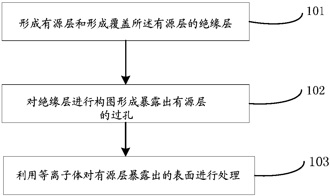
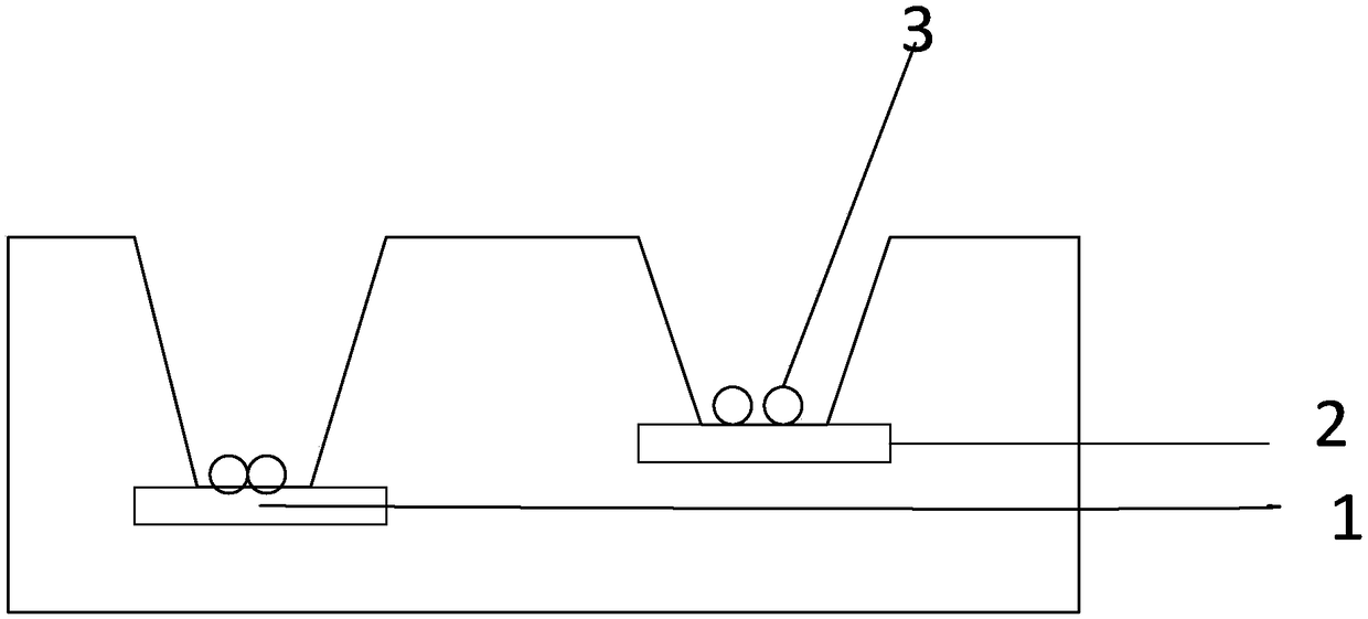
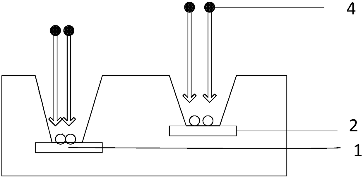
[0029] The embodiment of the present invention discloses a method for manufacturing a thin film transistor, which includes the steps of forming an active layer and the step of forming an insulating layer covering the active layer, and the manufacturing method further includes: After forming the via holes exposing the active layer by patterning, the exposed surface of the active layer is treated with plasma to remove organic impurities and / or oxides on the surface of the active layer.

[0030] The manufacturing method of the thin film transistor of the present invention can be found in figure 1 A brief flowchart is shown. The manufacturing m...


PUM


Abstract

The invention relates to the field of display, and particularly relates to a method manufacturing for a thin film transistor, a manufacturing method for the display substrate and a display device. Themanufacturing method of the thin film transistor comprises the steps of forming an active layer and forming an insulating layer covering the active layer, after the insulating layer is patterned, thethrough-hole of the active layer is exposed, treating the exposed surface of the active layer with plasma to remove organic impurities and / or oxides on the surface of the active layer. The manufacturing method of the thin film transistor adopts a dry method to process organic impurities on the surface of the active layer, avoids the pollution of the liquid medicine and improves the stability of the performance of the product. For the thin film transistor with the metal oxide as the active layer, the damage to the metal oxide can be avoided, and the management and the control of the product can be completed under the small uniformity variation.

Description

technical field [0001] The invention relates to the display field, in particular to a manufacturing method of a thin film transistor, a manufacturing method of a display substrate and a display device. Background technique [0002] OLED display panels have an array of pixels based on organic light emitting diodes. Each pixel includes an organic light emitting diode and a thin film transistor for controlling application of a signal to the organic light emitting diode. [0003] The manufacturing process of a thin film transistor is generally: depositing different film layers sequentially, such as a gate, a gate insulating layer, an active layer, a source electrode, and a drain electrode. The source and drain are in contact with the active layer. When the active layer is covered with an insulating layer, the source and drain electrodes are in contact with the active layer through the via holes. After the via hole is formed, in order to avoid impurities on the surface of the ...

Claims


Application Information

Patent Timeline
IPC IPC(8): H01L21/77H01L27/12
CPCH01L27/1225H01L27/1259H01L27/127
Inventor 王承贤杨静
Owner MIANYANG BOE OPTOELECTRONICS TECH CO LTD
Why Eureka
Try Eureka