Low-temperature polycrystal silicon thin film transistor and manufacturing method thereof

A technology of thin-film transistors and low-temperature polysilicon, which is applied in the direction of transistors, semiconductor/solid-state device manufacturing, semiconductor devices, etc., can solve problems such as increased heat generation and unfavorable product reliability, and achieve low power consumption, good heat dissipation, and reduced channels The effect of width

Inactive Publication Date: 2018-07-27
WUHAN CHINA STAR OPTOELECTRONICS SEMICON DISPLAY TECH CO LTD
View PDF5 Cites 1 Cited by
  • Summary
  • Abstract
  • Description
  • Claims
  • Application Information

AI Technical Summary

Problems solved by technology

[0003] However, while LTPS TFT has high electron mobility, its calorific value also increases, which is not conducive to improving product reliability.

Method used


Image

  • Low-temperature polycrystal silicon thin film transistor and manufacturing method thereof
  • Low-temperature polycrystal silicon thin film transistor and manufacturing method thereof
  • Low-temperature polycrystal silicon thin film transistor and manufacturing method thereof

Examples


Embodiment Construction

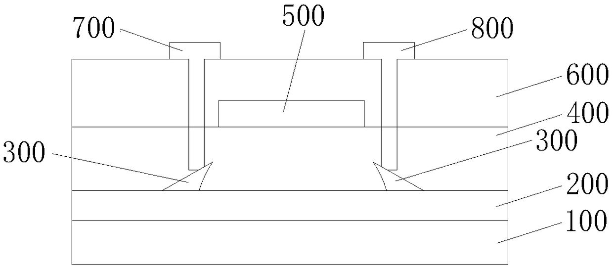
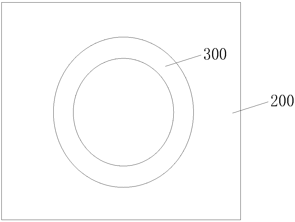
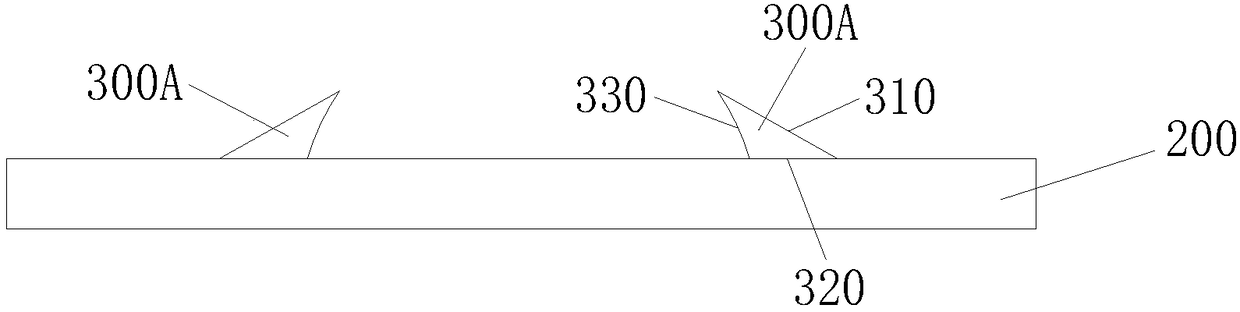
[0023] Hereinafter, embodiments of the present invention will be described in detail with reference to the accompanying drawings. This invention may, however, be embodied in many different forms and should not be construed as limited to the specific embodiments set forth herein. Rather, the embodiments are provided to explain the principles of the invention and its practical application, thereby enabling others skilled in the art to understand the invention for various embodiments and with various modifications as are suited to particular intended uses.

[0024] In the drawings, the thicknesses of layers and regions are exaggerated for clarity. Like reference numerals refer to like components throughout the specification and drawings.

[0025] It will be understood that when an element such as a layer, film, region, or substrate is referred to as being "on" or "formed on" another element, it can be directly on or formed directly on the other element. , or intermediate elemen...


PUM


Abstract

The invention provides a low-temperature polycrystal silicon thin film transistor. The low-temperature polycrystal silicon thin film transistor comprises an annular-like polycrystal silicon layer on asubstrate, a first insulating layer on the substrate and the polycrystal silicon layer, a gate on the first insulting layer, a second insulating layer on the first insulating layer and the gate, anda source and a drain on the second insulating layer, wherein the source and the drain run through the second insulating layer and the first insulating layer respectively to be in contact with the polycrystal silicon layer separately. The invention also provides a manufacturing method of the low-temperature polycrystal silicon thin film transistor. By manufacturing the annular-like polycrystal silicon layer, the channel width of the transistor can be reduced, thereby facilitating heat dissipation of the transistor, improving stability of the transistor, and further facilitating preparation of the high-resolution and low-power-consumption display panel.

Description

technical field [0001] The invention belongs to the technical field of manufacturing thin film transistors, and in particular relates to a low-temperature polysilicon thin film transistor and a manufacturing method thereof. Background technique [0002] At present, amorphous silicon thin-film transistors (a-Si TFTs) are widely used as switching elements of display panels, but a-Si TFTs meet the requirements of thin, light weight, high fineness, high brightness, high reliability, and low power consumption. and other requirements are still limited. Compared with the a-Si TFT, the Low Temperature Polycrystalline Silicon (LTPS) TFT has a polycrystalline silicon layer with high electron mobility, so it has obvious advantages in meeting the above requirements. [0003] However, while the LTPS TFT has high electron mobility, its calorific value also increases, which is not conducive to improving the reliability of the product. Contents of the invention [0004] In order to achi...

Claims


Application Information

Patent Timeline
Patent Type & Authority Applications(China)
IPC IPC(8): H01L29/10H01L29/786H01L21/336
CPCH01L29/1037H01L29/66757H01L29/78675H01L29/78696
Inventor 易国霞
Owner WUHAN CHINA STAR OPTOELECTRONICS SEMICON DISPLAY TECH CO LTD
Why Eureka
Try Eureka