
Organic light emitting display panel and manufacturing method thereof

a technology of light-emitting display panels and organic materials, applied in the field of display, can solve the problems of adversely affecting the improvement of product quality, the ineffectiveness of display devices, etc., and achieve the effects of reducing the width of the passage, preventing the penetration of outside moisture, and avoiding the reduction of the lifespan of products

Inactive Publication Date: 2021-10-28
WUHAN CHINA STAR OPTOELECTRONICS SEMICON DISPLAY TECH CO LTD
View PDF0 Cites 0 Cited by
  • Summary
  • Abstract
  • Description
  • Claims
  • Application Information

AI Technical Summary

Benefits of technology

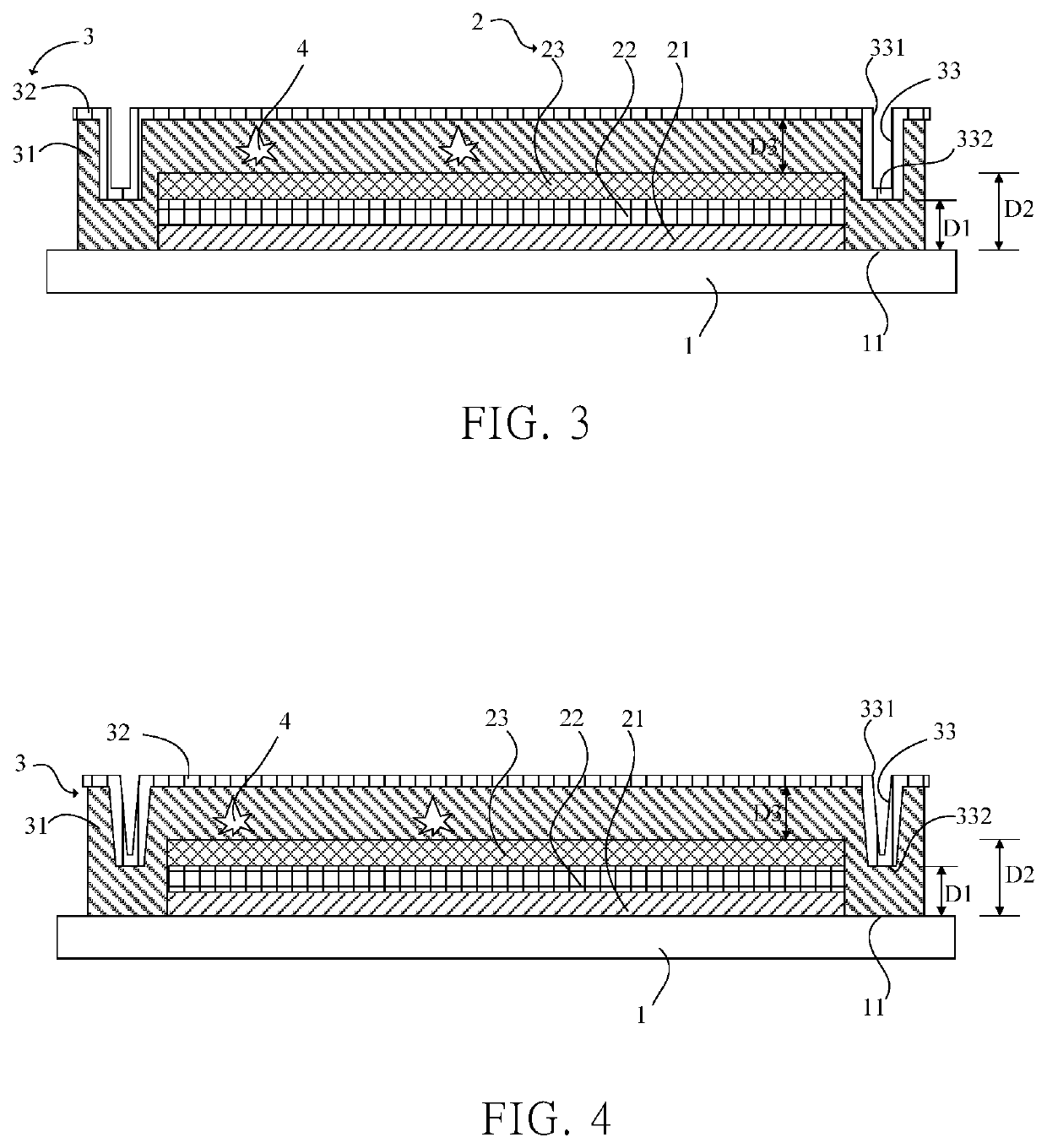
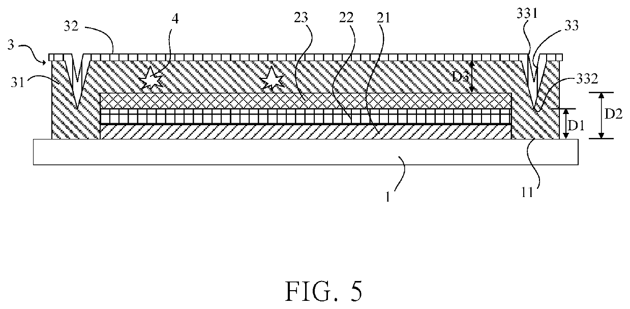
The present invention provides an organic light emitting display panel and a manufacturing method that improves encapsulation and reduces the thickness and width of the encapsulation film and moisture passage, thereby preventing damage to the light emitting layer from foreign matter and improving tolerance to foreign matter. The space between the metal film and organic light emitting module is enough to accommodate foreign matter and improve tolerance to foreign matter. The organic light emitting display panel effectively overcomes the drawbacks of traditional encapsulation structure that moisture easily permeates and foreign matter tends to damage the light emitting layer.

Problems solved by technology

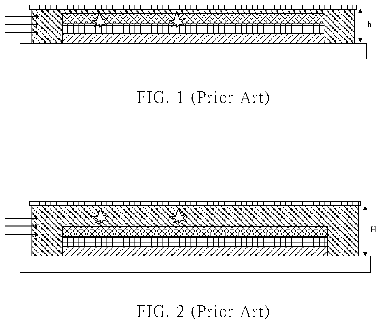
When a backplate is laminated with a metal film in the lamination processing chamber, remaining foreign matter in a resin film gap h, and affected by pressure, may damage an electroluminescence (EL) layer, and therefore forming a passage where moisture can permeate through, resulting in ineffectiveness of a display device.
In addition, an OLED device might be damaged by the pressure, and thus give rise to the occurrence of abnormal dark spots, thereby adversely affecting improvement of product quality.

Method used


Image

  • Organic light emitting display panel and manufacturing method thereof
  • Organic light emitting display panel and manufacturing method thereof
  • Organic light emitting display panel and manufacturing method thereof

Examples


Embodiment Construction

[0027]The following embodiments are referring to the accompanying drawings for exemplifying specific implementable embodiments of the present disclosure. Furthermore, directional terms described by the present disclosure, such as upper, lower, front, back, left, right, inner, outer, side, etc., are only directions by referring to the accompanying drawings, and thus the used directional terms are used to describe and understand the present disclosure, but the present disclosure is not limited thereto. In the drawings, elements with similar structures are labeled with like reference numerals.

[0028]An organic light emitting display panel of the present invention is exemplified as an organic light emitting diode (OLED) display panel. FIG. 3 is a schematic cross-sectional view of an organic light emitting display panel in accordance with an embodiment of the present invention. The organic light emitting display panel includes a backplate 1, an organic light emitting module 2, and an enca...


PUM

PropertyMeasurementUnit
distanceaaaaaaaaaa
aperture widthaaaaaaaaaa
shapeaaaaaaaaaa

Abstract

An organic light emitting display panel includes a backplate, an organic light emitting module disposed on the backplate, and a lip portion of the backplate is defined between an edge of the backplate and an edge of the organic light emitting module. An encapsulation layer is configured to encapsulate the backplate and the organic light emitting module and cover the lip portion. The encapsulation layer includes an encapsulation resin film laminated on the backplate and a metal film disposed on the encapsulation resin film. The metal film extends toward the backplate and bends inwardly within the encapsulation resin film on the lip portion of the backplate to form a groove.

Description

BACKGROUND OF INVENTION1. Field of Invention[0001]The present invention relates to a display field, and particularly to an organic light emitting display panel and a manufacturing method thereof capable of improving encapsulation effect,2. Related Art[0002]In recent years, with ongoing development of display technology, organic light emitting diode (OLED) devices, as a new display technology, have attracted wide attention due to advantages of being self-luminous, wide viewing angles, high resolution, and low power consumption. In the manufacturing process of OLED displays, surface encapsulation technology has been widely used as the mainstream encapsulation technology for current OLED displays. Particularly, metal encapsulation dominates the market because of its good moisture barrier properties and contribution to achieve compact configuration of products.[0003]Conventionally, due to the limitation of the moisture barrier properties, resin films used in metal encapsulation technolo...

Claims


Application Information

Patent Timeline
Patent Type & Authority Applications(United States)
IPC IPC(8): H01L51/52H01L51/56
CPCH01L51/5253H01L51/56H10K59/8722H10K59/8721H10K50/844H10K71/00
Inventor LIU, JIE
Owner WUHAN CHINA STAR OPTOELECTRONICS SEMICON DISPLAY TECH CO LTD
Learn More