Carrier and substrate manufacturing method using this carrier
A manufacturing method and carrier technology, which is applied in the fields of record carrier manufacturing, semiconductor/solid-state device manufacturing, manufacturing tools, etc., and can solve problems such as damage to the substrate substrate surface
- Summary
- Abstract
- Description
- Claims
- Application Information
AI Technical Summary
Problems solved by technology
Method used
Image

Examples
no. 1 Embodiment approach
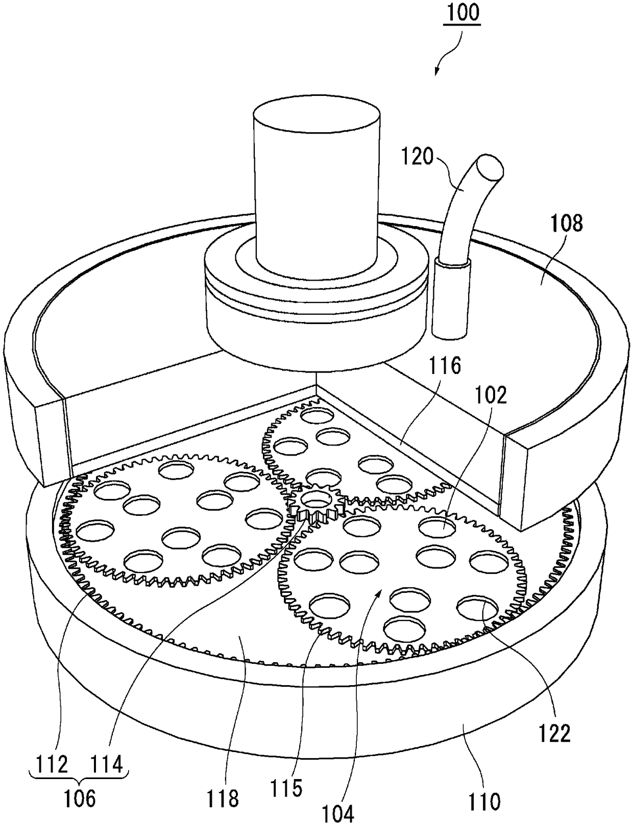
[0053] figure 1 It is a figure which shows the cross section of the main part of the double-side polishing apparatus used when polishing the surface of the board|substrate of this embodiment. In addition, in this embodiment, only the double-sided grinding device is described, but it is not limited thereto. For example, the grinding pad provided on the platen is changed to a grinding pad, and it can also be used as a double-sided grinding device having the same function. .
[0054] As the substrate (to-be-processed object), for example, an annular or square plate-shaped substrate can be used. Specific examples of these substrates include substrates for magnetic disks such as substrates made of glass or aluminum alloys, aluminum alloy substrates with a NiP alloy coating film formed on the surface, rectangular glass substrates for liquid crystal panels, and glass for screen protection. cover, photomask base, silicon wafer, etc., but the material, shape, size, etc. of the substr...
Embodiment
[0103] Hereinafter, examples of the present invention will be described by way of example, but the present invention is not limited to the following examples.
[0104] (Preparation of substrate to be processed)
[0105] The substrate to be processed was set as a glass substrate for a magnetic disk with a nominal size of 2.5 (about 65 mm in diameter), and the following substrate was prepared by a known method. owned.
[0106] (Preparation of the carrier for the experiment)
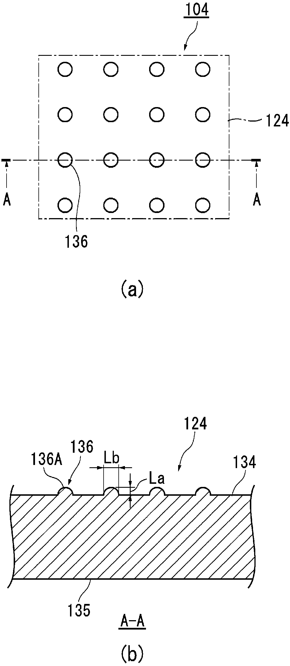
[0107] The carrier was manufactured by shape-processing a sheet obtained by weaving glass fibers and impregnating epoxy resin. Then, using the method described above as appropriate, additional processing was performed on one surface of the carrier to form a plurality of protrusions having the specifications shown in Table 1. In addition, regarding other specifications, the width of the protrusions is set to 300 μm, and the density of the protrusions is set to 3 (pcs / mm 2 ), and the proportion of the are...
no. 2 Embodiment approach
[0136] A second embodiment of the carrier of the present invention and a method of manufacturing a substrate using the carrier will be described. The parts that overlap with the description of the above-mentioned first embodiment are given the same reference numerals and the description thereof will be omitted.
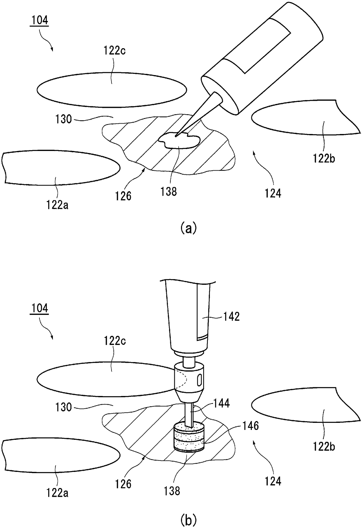
[0137] Image 6 is showing figure 1 A top view of the carrier 104. On the upper surface 124 of the carrier 104 representatively shown in the figure, recesses 128 are provided in a plurality of regions 126 (protrusion forming regions) (refer to Figure 7 (b)). As shown, the plurality of regions 126 are located outside the perimeter 130 of the retaining aperture 122 and are spaced apart from one another. In particular, it may be a region surrounded by at least three holding holes 122 and not continuous with the holding holes 122 .
[0138] In addition, the contour forming the plurality of concave portions 128 is formed of a free curve, for example, formed so as not...
PUM
| Property | Measurement | Unit |
|---|---|---|
| Height | aaaaa | aaaaa |
| Width | aaaaa | aaaaa |
| Depth | aaaaa | aaaaa |
Abstract
Description
Claims
Application Information
PatSnap Eureka turns technology decisions into work you can execute. Powered by our Innovation Knowledge Graph, it runs expert workflows across engineering, life sciences, materials and intellectual property. Get your review-ready output in minutes.


