Two-way positive-end current sampling module and circuit, switch circuit and current sampling method

A current sampling and switching circuit technology, which is applied in the direction of electronic switching, measuring current/voltage, measuring electricity, etc., can solve the problems of low precision, inability to guarantee the consistency of output branch current sampling, complex sampling circuit structure, etc., to ensure consistency The effect of realizing high-precision multi-channel positive terminal current sampling

Pending Publication Date: 2018-08-03
WUXI SI POWER MICRO ELECTRONICS
0 Cites 2 Cited by

AI-Extracted Technical Summary

Problems solved by technology

[0003] The purpose of the present invention is to overcome the deficiencies in the prior art, to provide a dual-channel positive-terminal current sampling module, and a dual-channel positive-terminal current sampling circuit and a switch circuit based o...

Abstract

The invention provides a two-way positive-end current sampling module. According to the two-way positive-end current sampling module, one end of a resistor R5 is connected to a source electrode of a PMOS tube MP1, a source electrode of a PMOS tube MP4 and a source electrode of a PMOS tube MP5; one end of a resistor R6 is connected to a source electrode of a PMOS tube MP2; one end of the resistor R7 is connected to a source electrode of a PMOS tube MP3; a grid electrode of the PMOS tube MP1 is connected with a grid electrode of the PMOS tube MP2, a grid electrode of the PMOS tube MP3 and a drain electrode of MP1; a drain electrode of the PMOS tube MP1 is connected with a chip through a current source IS1, a drain electrode of the PMOS tube MP2 is connected with the chip through a current source IS2, and a drain electrode of the PMOS tube MP3 is connected with the chip through a current source IS2; a grid electrode of the PMOS tube MP4 is connected with the drain electrode of the PMOS tube MP2, and a grid electrode of the PMOS tube MP5 is connected with the drain electrode of the PMOS tube MP3; a drain electrode of the PMOS tube MP4 and a drain electrode of the PMOS tube MP5 are connected with one end of a resistor R8, and the other end of the resistor R8 is connected with the chip; one end of the resistor R8 is used for outputting voltage feedback signals VSEN. By the adoption of the two-way positive-end current sampling module, two-way high-accuracy current sampling is achieved.

Application Domain

Electrical measurement instrument detailsElectrical testing +2

Technology Topic

EngineeringCurrent source +3

Image

  • Two-way positive-end current sampling module and circuit, switch circuit and current sampling method
  • Two-way positive-end current sampling module and circuit, switch circuit and current sampling method
  • Two-way positive-end current sampling module and circuit, switch circuit and current sampling method

Examples

  • Experimental program(1)

Example Embodiment

[0030] The present invention will be further described below in conjunction with specific drawings and embodiments.
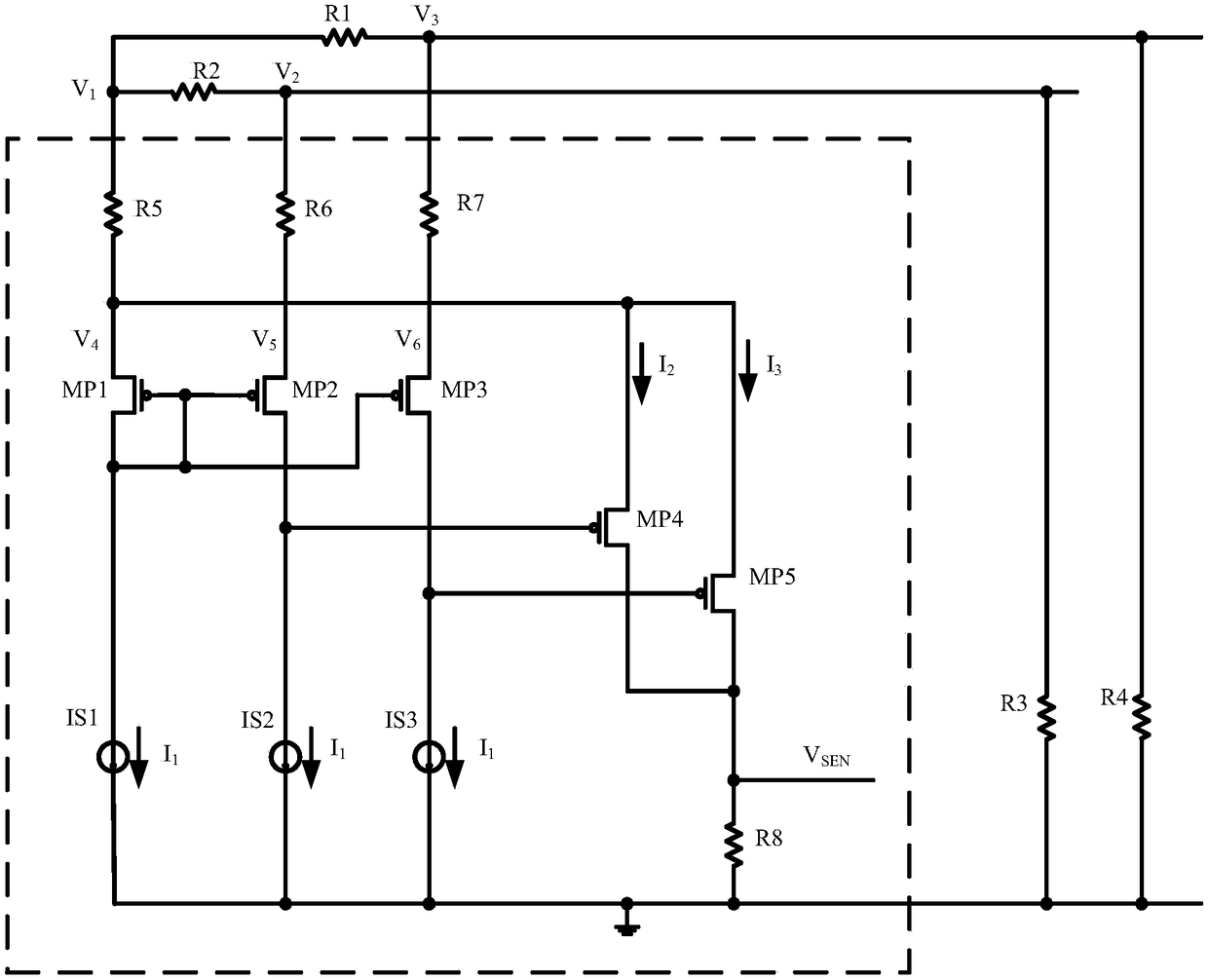
[0031] The invention provides a high-precision dual-channel positive-end current sampling module, and a dual-channel positive-end current sampling circuit such as figure 1 As shown; the dashed frame part is a dual-channel positive-end current sampling module, which can be made into a chip;
[0032] The dual-channel positive-end current sampling module includes resistors R5, R6, R7 with the same resistance, the same PMOS tubes MP1, MP2, MP3, the same PMOS tubes MP4 and MP5, resistance R8, and current sources IS1, IS2, IS3 with the same current ; Among them, MP1, MP2, MP3 are low-voltage PMOS tubes, MP4 and MP5 are thin-gate oxygen high-voltage PMOS tubes; outside the dashed box are the peripheral components of the chip, which form a dual positive-end current sampling circuit with the chip; among them, R1 and R2 are respectively High-precision sampling resistors on the two output branches, R3 and R4 are the loads on the two output branches respectively;
[0033] One end of the resistor R5 is connected to the source of the PMOS tube MP1, the source of the PMOS tube MP4, and the source of the PMOS tube MP5; one end of the resistance R6 is connected to the source of the PMOS tube MP2; one end of the resistance R7 is connected to the source of the PMOS tube MP3; The gate of the PMOS tube MP1 is connected to the gate of the PMOS tube MP2, the gate of the PMOS tube MP3 and the drain of the MP1; the drain of the PMOS tube MP1 is connected to the chip ground through the current source IS1, and the drain of the PMOS tube MP2 is connected through the current source IS2 Connected to chip ground, the drain of PMOS tube MP3 is connected to chip ground through current source IS2; the gate of PMOS tube MP4 is connected to the drain of PMOS tube MP2, and the gate of PMOS tube MP5 is connected to the drain of PMOS tube MP3; PMOS tube MP4 and The drain of MP5 is connected to one end of resistor R8, the other end of resistor R8 is connected to chip ground; one end of resistor R8 is used to output voltage feedback signal V SEN; The currents of the current sources IS1, IS2, IS3 are all I 1;
[0034] A high-precision dual-channel positive-end current sampling circuit includes a first output branch, a second output branch, and the above-mentioned dual-channel positive-end current sampling module; the first output branch includes a sampling resistor R1 and a load R4. The second output branch includes sampling resistor R2 and load R3;
[0035] One end of the sampling resistors R1 and R2 is connected together and connected to the other end of the resistor R5. The one end of the sampling resistors R1 and R2 connected is the common end of the sampling resistor; the other end of the sampling resistor R2 is connected to the other end of the resistor R6 and the load R3. One end; the other end of the sampling resistor R1 is connected to the other end of the resistor R7 and one end of the load R4; the other ends of the loads R3 and R4 are grounded, and the chip ground of the dual positive-end current sampling module is also grounded.
[0036] The working principle and related formula derivation of the high-precision dual-channel positive-end current sampling circuit will be explained in detail below. The voltage of each node and the current of each branch are as figure 1 Marked in; figure 1 Since MP1, MP2, and MP3 are the same, the channel modulation effect is ignored. Assuming that both MP4 and MP5 have current, MP1~MP3 all work in the saturation region. Combining the saturation region formula of the MOS tube, it is easy to know that V4=V5=V6, and get The following equation:
[0037] V 1 -(I 1 +I 2 +I 3 )*R 5 =V 2 -I 1 *R 6 (1)
[0038] V 1 -(I 1 +I 2 +I 3 )*R 5 =V 3 -I 1 *R 7 (2)
[0039] As R 5 =R 6 =R 7 , So get:
[0040] V 1 -V 2 =(I 2 +I 3 )*R 5 (3)
[0041] V 1 -V 3 =(I 2 +I 3 )*R 5 (4)
[0042] When V 1 -V 2 And V 1 -V 3 When equal, I 2 And I 3 Can be any combination, suppose I 3 =0, then:
[0043]
[0044] When V 1 -V 2 And V 1 -V 3 When they are not equal, combining formulas (3) and (4) shows that if MP4 and MP5 have incorrect currents, only one of the two can be turned on, the other is in the off state, and the PMOS transistor MP4 or MP5 in the off state The PMOS tube connected to the gate works in the linear region. Reasoning easily V 1 -V 2 And V 1 -V 3 The PMOS tube MP4 or MP5 corresponding to the output branch with a large medium pressure difference is turned on. For example V 1 -V 2V 1 -V 3 , MP2 works in the saturation region, MP3 works in the linear region, MP4 is turned on and current flows through, and MP5 is in the off state, that is, I3=0, then
[0045]
[0046] Based on the above analysis and formulas (5) and (6), it can be seen that the double-channel positive-end current sampling module in the dashed box can compare and filter the two output branches with a large voltage difference between the two output branches. And convert the load current signal into a voltage feedback signal V SEN Passed to the next module, the ratio of R8 to R5 is the amplification factor of the load current signal. The sampling formula of the dual-channel positive-end current sampling module is as follows:
[0047]
[0048] The ratio of the resistors R8 and R5 can be used to adjust the amplification factor of the sampling circuit, and the resistance type of the resistors R8 and R5 can be used to adjust the temperature coefficient of the sampling circuit.
[0049] It can be deduced from the formula that as long as the absolute matching of the first detection branch circuit (R6, MP2, IS2 and MP4) and the second detection branch circuit (R7, MP3, IS3 and MP5) is ensured, the double positive terminal The current sampling circuit can achieve exactly the same current sampling coefficient, so the actual design process also needs to consider the impact of process mismatch. Considering that in the process of production, the parameter control of low-voltage devices is much easier than that of high-voltage devices, and higher accuracy can be achieved. Therefore, MP1~MP3 in this circuit adopt low-voltage tubes, in order to further weaken the influence of channel modulation effect MP1~MP3 The gate length of is recommended to be more than 5μm; in order to improve the matching degree and reduce the influence of mismatch, the gate width is also recommended to be more than 5μm.
[0050] In summary, the current sampling method proposed in the present invention includes:
[0051] Set two output branches, including a first output branch and a second output branch; the first output branch includes a sampling resistor R1 and a load R4, and the second output branch includes a sampling resistor R2 and a load R3; a sampling resistor R1 and One end of R2 is connected together as the common end of the sampling resistor; the sampling resistor R1 is connected in series with the load R4, and the sampling resistor R2 is connected in series with the load R3;
[0052] Detect the positive terminal voltage of the common terminal of the sampling resistor to obtain the positive terminal voltage feedback signal that characterizes the output current information;
[0053] Detecting the negative terminal voltage of the sampling resistor in the first output branch to obtain a negative terminal voltage feedback signal representing output current information of the first output branch;
[0054] Detecting the negative terminal voltage of the sampling resistor in the second output branch to obtain a negative terminal voltage feedback signal representing the output current information of the second output branch;
[0055] By comparing the voltage feedback voltage difference signal on the sampling resistors in the two output branches, the output current information of the output branch with the larger voltage difference is converted into the voltage feedback signal V SEN , Passed to the next level to achieve overcurrent protection or constant current function;
[0056] The switch circuit provided by the present invention is such as figure 2 Shown, including: switch tube M1, rectifier tube M2, inductor L, output capacitor Cout, dual positive-end current sampling module, sampling resistors R1, R2, feedback resistors R23, R24, loads R3, R4, drive circuit 21, RS Flip-flop 22, PWM comparator 23, operational amplifier 24, level selection circuit 25, compensation resistor R25, compensation capacitor C21; among them, the switch tube M1 and the rectifier tube M2 are NMOS tubes, and the RS flip-flop 22 is valid for high-level input;
[0057] The drain of the switch M1 is connected to the input voltage signal V IN , The gate is connected to one output end of the drive circuit 21, the other output end of the drive circuit 21 is connected to the gate of the rectifier M2; the source of the rectifier M2 is grounded; the source of the switch M1 is connected to the drain of the rectifier M2 and One end of the inductor L, the other end of the inductor L is connected to one end of the output capacitor Cout, and one end of the sampling resistors R1 and R2; the other end of the output capacitor Cout is grounded; the other end of the resistor R5 in the dual positive-end current sampling module is connected to the sampling resistor One end of R1 and R2, the other end of resistor R6 in the dual-channel positive-end current sampling module is connected to the other end of sampling resistor R2, and the other end of resistor R7 in the dual-channel positive-end current sampling module is connected to the other end of sampling resistor R1; The other end of R1 is grounded through load R4; the other end of sampling resistor R2 is connected to one end of feedback resistor R23 and grounded through load R3; the other end of feedback resistor R23 is grounded through feedback resistor R24; the chip ground of the dual positive-end current sampling module is grounded ;
[0058] The voltage feedback signal V obtained from the dual positive terminal current sampling module SEN And the voltage feedback signal V obtained from the connection node of the feedback resistors R23 and R24 FB The level selection circuit 25 is respectively input, and the level selection circuit 25 compares the voltage feedback signal V SEN And V FB The size of V SEN And V FB The larger signal is transmitted to the inverting input terminal of the operational amplifier 24; the non-inverting input terminal of the operational amplifier 24 is connected to the reference voltage V REF; The output terminal of the operational amplifier 24 is connected to the inverting input terminal of the PWM comparator 23, and the non-inverting input terminal of the PWM comparator is connected to the triangular wave signal V ramp; The output terminal of the PWM comparator 23 is connected to the R terminal of the RS flip-flop 22, and the S terminal of the RS flip-flop 22 is connected to the pulse signal V pulse The Q terminal of the RS flip-flop 22 is connected to the input terminal of the driving circuit 21.
[0059] More preferably, the output terminal of the operational amplifier 24 is also grounded through a compensation resistor R25 and a compensation capacitor C21 connected in series.
[0060] in figure 2 Medium, V out Is the positive terminal voltage of the common terminal of the sampling resistor, V SEN1 Is the negative terminal voltage of the sampling resistor R1 in the first output branch, V SEN2 Is the negative terminal voltage of the sampling resistor R2 in the second output branch, and the dual positive terminal current sampling module compares V out -V SEN1 And V out -V SEN2 Then convert the larger difference value into a voltage feedback signal V SEN; Passed to the level selection circuit 25, the level selection circuit 25 through the comparison voltage feedback signal V SEN And V FB The size of V SEN And V FB The larger signal is passed to the inverting input terminal of the operational amplifier 24 and participates in the loop control of the circuit; signal V SEN Greater than V FB When the constant voltage loop (the loop where the feedback resistors R23, R24 and the level selection circuit 25 are located) is shielded, the constant current loop (sampling resistors R1, R2, dual positive-end current sampling modules, and the level selection circuit The loop where 25 is located) works, and the load current has been stable at the set constant current point. Here, the constant current point is set by the dual-channel positive-end current sampling module and the high-precision sampling resistor R1 of the first output branch and the high-precision sampling resistor R2 of the second output branch. When VS EN Signal is less than V FB When the constant current loop is shielded, the constant voltage loop works, and the output voltage is always stable at the set value. Here the output voltage is determined by the reference voltage V REF , The feedback resistance R23 and the feedback resistance R24 are set.
[0061] Combine below image 3 The timing diagram of the constant current/constant voltage working mode is given to introduce the working principle of this topology. Before t1, the load current i of the first output branch out1 Less than the constant current point, the load is small, the load current i of the second output branch out2 Is 0. At this time, the V sampled by the dual positive terminal current sampling module SEN The voltage is small, less than V FB , The constant current loop is shielded, the constant voltage loop works, V FB The level is adjusted and stabilized at the reference voltage V through the constant voltage loop REF Up and down, output voltage V out Constant. At t1, the load of the first output branch suddenly switches to a constant voltage source, and the output voltage is V out Was pulled down. At this time V FB The same ratio is reduced, and the upper tube M1 is controlled to be turned on for a long time through the constant voltage loop to provide sufficient energy to the output. With the load current i of the first output branch out1 Gradually increase, the V sampled by the dual positive terminal current sampling module SEN The voltage also gradually rises, when V SEN Voltage is higher than V FB When the constant voltage loop is shielded, the constant current loop starts to control the entire loop, and finally the load current i of the first output branch out1 Stable at constant current point, output voltage V out Same as the constant voltage source load of the first output branch.
[0062] Although the present invention has been described with reference to the exemplary embodiments, it should be understood that the terms used are illustrative and exemplary, and not restrictive terms. Since the present invention can be implemented in various forms without departing from the spirit or essence of the invention, it should be understood that the foregoing embodiments are not limited to any of the foregoing details, but should be broadly understood within the spirit and scope defined by the claims. Therefore, all changes and modifications falling within the scope of the claims or their equivalents shall be covered by the appended claims.

PUM

no PUM

Description & Claims & Application Information

We can also present the details of the Description, Claims and Application information to help users get a comprehensive understanding of the technical details of the patent, such as background art, summary of invention, brief description of drawings, description of embodiments, and other original content. On the other hand, users can also determine the specific scope of protection of the technology through the list of claims; as well as understand the changes in the life cycle of the technology with the presentation of the patent timeline. Login to view more.

Similar technology patents

Pneumatic seeder

InactiveCN103168537AEnsure consistency
Owner:马强

System and method for detecting intelligent key

ActiveCN103280006AEnsure consistency
Owner:上海纳恩汽车技术股份有限公司

Titanium alloy bar billet drawing-out forging method

ActiveCN108262435AEnhanced deformation controllabilityEnsure consistency
Owner:AVIC BEIJING INST OF AERONAUTICAL MATERIALS

Private network frequency-selecting networking chain building method based on short wave channel

ActiveCN106658529AEnsure consistencyImprove channel quality
Owner:中国人民解放军国防信息学院

A power module structure capable of improving welding quality

ActiveCN105280565AEnsure consistencyPrevent drifting and tilting
Owner:NANJING HIGHSEMI ELECTRIC POWER SCI & TECH CO LTD

Classification and recommendation of technical efficacy words

  • Ensure consistency

Soybean milk machine with small-space crushing cover

ActiveCN103654475AImproved material crushing effectEnsure consistency
Owner:JOYOUNG CO LTD

Testing system for mobile terminal and testing method thereof

Owner:广东每通测控科技股份有限公司

3D printing device and method

ActiveCN104960202AEnsuring Quality and ConsistencyEnsure consistency
Owner:HUAZHONG UNIV OF SCI & TECH

Automatic test method based on case library

InactiveCN104572449AEnsure consistencyImprove coverage and test efficiency
Owner:CHINA MOBILE GRP GUANGDONG CO LTD
Why Eureka
Try Eureka