Screen, method for making area light source and method for making direct type backlight module

A manufacturing method and backlight module technology, applied to screen printing machines, rotary printing machines, printing, etc., can solve the problems of uniformity influence, light shape change, LED chip arrangement regularity deterioration, etc., to ensure uniformity Uniformity of light output, smooth and uniform contact surface, and improved uniformity of brightness

Active Publication Date: 2018-08-03
WUHAN CHINA STAR OPTOELECTRONICS TECH CO LTD
View PDF7 Cites 7 Cited by
  • Summary
  • Abstract
  • Description
  • Claims
  • Application Information

AI Technical Summary

Problems solved by technology

[0003] The surface light source is a type of direct-lit backlight. In the preparation process of the surface light source, a layer of solder paste needs to be brushed on the LED substrate with a screen, and the solder paste is evenly spread on the pads of the LED substrate. The uniformity of the LED chip array plays a vital role in the uniformity of the subsequent LED chip array. However, the existing screen structure is difficult to ensure the uniformity of the solder paste coating in the solder paste coating, the tolerance of the aperture size, the solder paste The direction of the scraping will affect the uniformity of the solder paste on the pad, so that the regularity of the arrangement of the LED chip on the LED substrate will be deteriorated, and the shape of the light will change. At the same time, the contact area between the LED chip and the solder paste will be different. Uniformity also leads to uneven brightness of the LED chip. In summary, the above two points lead to uneven brightness of the entire surface of the surface light source.

Method used


Image

  • Screen, method for making area light source and method for making direct type backlight module
  • Screen, method for making area light source and method for making direct type backlight module
  • Screen, method for making area light source and method for making direct type backlight module

Examples


Embodiment Construction

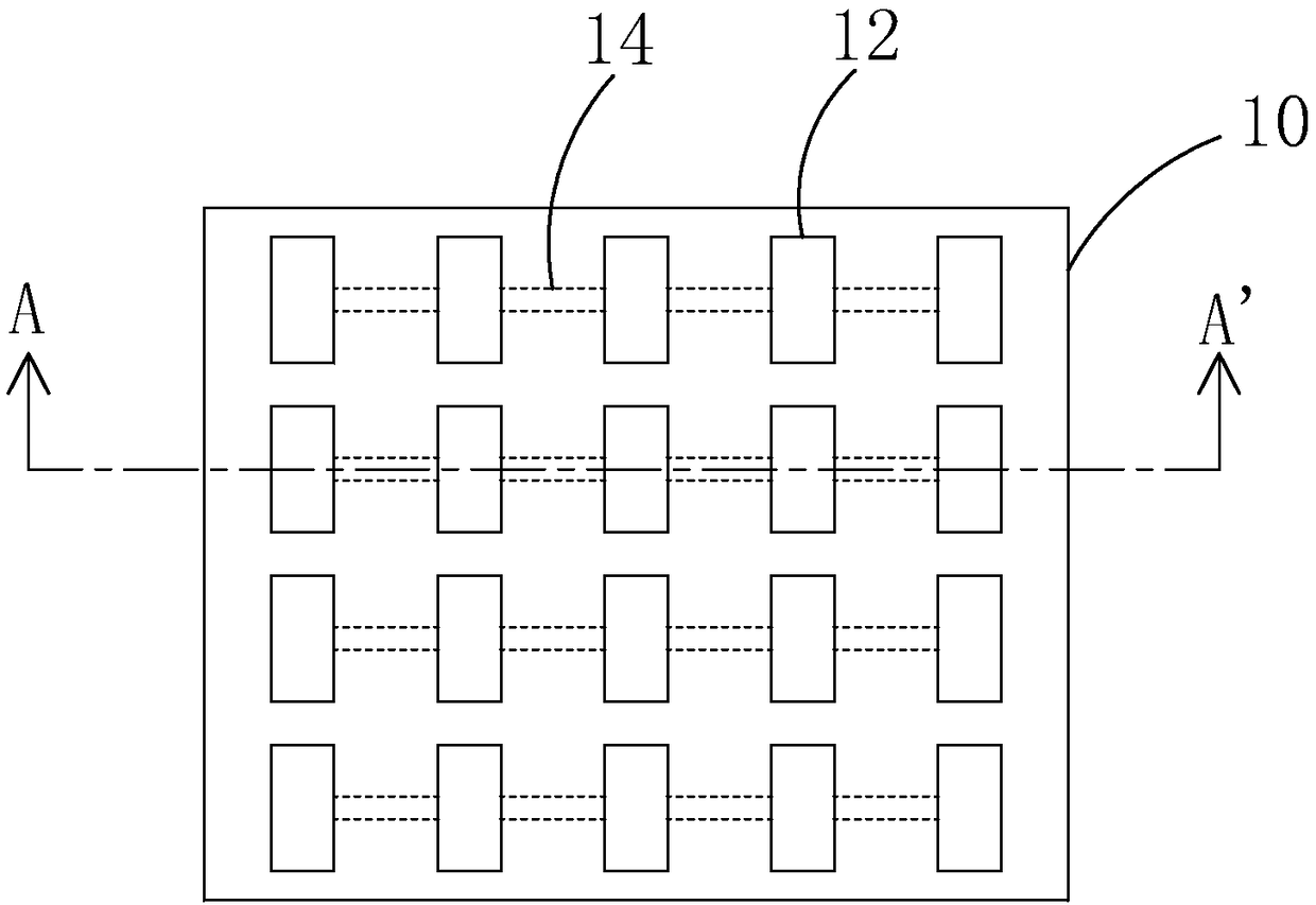
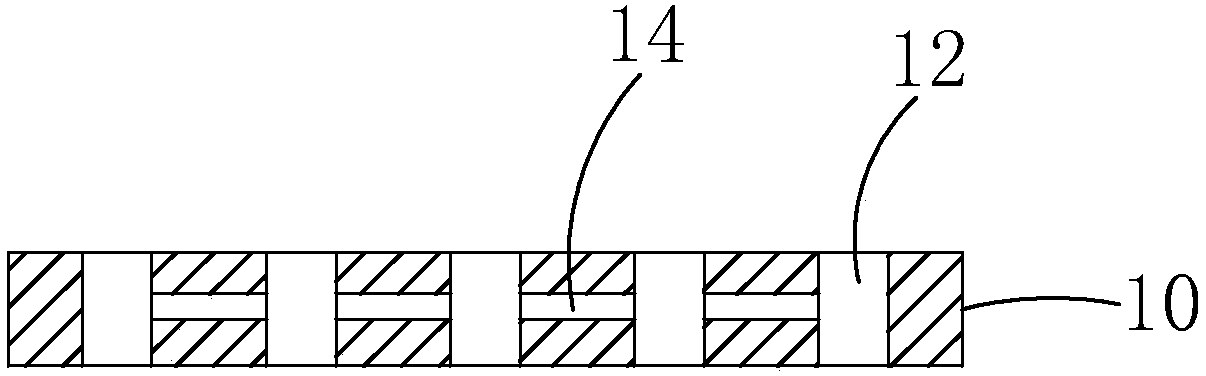
[0031] In order to further illustrate the technical means adopted by the present invention and its effects, the following describes in detail in conjunction with preferred embodiments of the present invention and accompanying drawings.

[0032] see figure 1 and figure 2 , the present invention provides a screen 10 for printing solder paste in cooperation with a scraper, provided with several openings 12 arranged at intervals and several communicating holes 14 respectively connected to adjacent openings 12 arranged along the scraping direction of the scraper , each communication hole 14 can balance the solder paste height between the two openings 12 adjacent to the communication hole 14 when applying solder paste.

[0033] Specifically, the opening 12 runs through the upper surface and the lower surface of the screen 10, and the communication holes 14 are located between the upper surface and the lower surface of the screen 10, that is, the plurality of communication holes 14...


PUM


Abstract

The invention provides a screen, a method for making an area light source and a method for making a direct type backlight module. The screen comprises a plurality of openings and a plurality of communicating holes, wherein the plurality of openings are formed at intervals; the plurality of communicating holes are respectively communicated with adjacent openings formed in a scrape coating directionof a scraper; when solder paste is coated, the solder paste height between two openings adjacent to the communicating hole can be balanced by the communicating hole, and the coating uniformity of thesolder paste is effectively ensured. The screen is used in the method for making the area light source, the communicating hole is formed between every two adjacent openings formed in the scrape coating direction of a scraper in the screen, and the moving direction of the communicating hole is the same as the scrape coating direction of the scraper, so that the solder paste amount on a bonding padof a MINI LED substrate is balanced by utilizing a principle of a similar connector, and the contact surface between the subsequent solder paste and a MINI LED chip is flat and uniform. Therefore, the arrangement uniformity and emergence uniformity of subsequent MINI LED chip arrangement are ensured, and the brightness uniformity of the whole area light source surface is improved.

Description

technical field [0001] The invention relates to the field of display technology, in particular to a method for manufacturing a screen plate, a surface light source, and a direct-type backlight module. Background technique [0002] With the development of display technology, liquid crystal display (Liquid Crystal Display, LCD) and other flat display devices are widely used in mobile phones, TVs, Various consumer electronic products such as personal digital assistants, digital cameras, notebook computers, and desktop computers have become the mainstream of display devices. Most of the liquid crystal display devices currently on the market are backlight liquid crystal display devices, which include a liquid crystal display panel and a backlight module (Backlight Module). The working principle of the liquid crystal display panel is to place liquid crystal molecules between two parallel glass substrates. There are many vertical and horizontal small wires between the two glass su...

Claims


Application Information

Patent Timeline
Patent Type & Authority Applications(China)
IPC IPC(8): H01L33/62H01L33/00B41F15/08
Inventor 杨勇张桂洋查国伟崔宏青
Owner WUHAN CHINA STAR OPTOELECTRONICS TECH CO LTD
Why Eureka
Try Eureka