Antenna device and method for manufacturing antenna device

A technology of antenna device and radome, which is applied in the direction of antenna, antenna coupling, electrical short antenna, etc., and can solve the problems of thinning and thinning wireless devices.

Active Publication Date: 2018-08-07
MURATA MFG CO LTD
View PDF15 Cites 3 Cited by
  • Summary
  • Abstract
  • Description
  • Claims
  • Application Information

AI Technical Summary

Problems solved by technology

[0006] In the wireless device disclosed in Patent Document 1, since it is necessary to secure a space between the wireless module and the case, it is difficult to make the wireless device thinner.

Method used


Image

  • Antenna device and method for manufacturing antenna device
  • Antenna device and method for manufacturing antenna device
  • Antenna device and method for manufacturing antenna device

Examples


no. 1 example

[0041] Reference Figure 1A to Figure 1D The drawings illustrate the antenna device of the first embodiment.

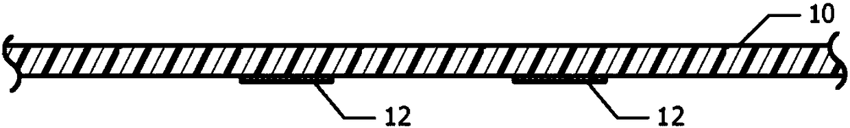
[0042] Figure 1A It is a partial cross-sectional view of the radome 10 and the passive element 12 used in the antenna device of the first embodiment. The radome 10 is, for example, a plate-shaped member made of a dielectric. A plurality of passive elements 12 are provided on one surface (inner surface) of the radome 10.

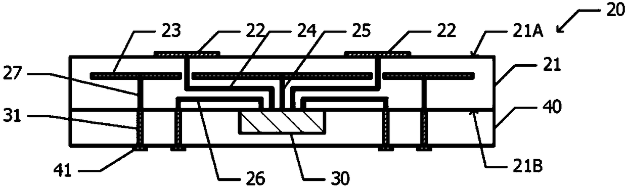
[0043] Figure 1B It is a cross-sectional view of the antenna module 20 used in the antenna device of the first embodiment. A plurality of power feeding elements 22 are formed on one surface (first surface) 21A of the dielectric substrate 21. For example, a patch antenna is used as the power supply element 22. The high-frequency integrated circuit element 30 is mounted on the second surface 21B of the dielectric substrate 21 on the side opposite to the first surface 21A. A ground plane 23 is arranged on the inner layer of the dielectric substrate 21....

no. 2 example

[0059] Next, the antenna device of the second embodiment will be described with reference to FIG. 3. Hereinafter, description of the configuration common to the antenna device of the first embodiment will be omitted.

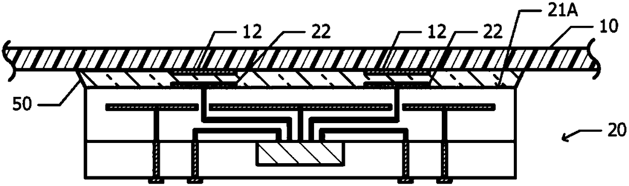
[0060] Figure 3A It is a cross-sectional view of the antenna module 20 used in the antenna device of the second embodiment. In the first embodiment, in the stage before bonding with the radome 10, such as Figure 1B As shown, the power supply element 22 of the antenna module 20 is exposed. In the second embodiment, the first surface 21A of the dielectric substrate 21 and the power supply element 22 are covered by the dielectric layer 28. In this way, the power feeding element 22 is not arranged on the surface of the antenna module 20 but on the inner layer.

[0061] Figure 3B It is a cross-sectional view of the antenna device of the second embodiment. An adhesive layer 50 is arranged between the dielectric layer 28 of the antenna module 20 and the radome 10. As...

no. 3 example

[0065] Next, refer to Figure 4A with Figure 4B The antenna device of the third embodiment will be described. Hereinafter, description of the configuration common to the antenna device of the first embodiment will be omitted.

[0066] Figure 4A It is a cross-sectional view of the antenna device of the third embodiment. In the third embodiment, the convex portion 11 is provided on the inner surface of the radome 10. The antenna module 20 is in contact with the side surface (step surface) 11A of the convex portion 11.

[0067] Figure 4B It is a top view of the antenna device of the third embodiment. Figure 4B The one-dot chain line 4A-4A is equivalent to Figure 4A Cutaway view. The antenna module 20 has a substantially rectangular planar shape. The convex portions 11 provided on the inner surface of the radome 10 are arranged at positions corresponding to the four corners of the antenna module 20. The four corners of the antenna module 20 are chamfered to match the step surf...


PUM


Abstract

The invention provides an antenna device, which is suitable for thinning and lightening an apparatus and is not liable to cause staggering between a power supply component and a passive component. Anantenna module includes a dielectric substrate and a feed element provided on the dielectric substrate. A radome formed from a dielectric is disposed so as to oppose the antenna module in a radiationdirection of the feed element. A parasitic element is provided at a position on the radome at which the electromagnetic coupling with the feed element is achieved. The antenna module is bonded to theradome by an adhesive layer disposed between the antenna module and the radome.

Description

Technical field [0001] The present invention relates to an antenna device and a manufacturing method of the antenna device. Background technique [0002] A wireless device including a substrate, a wireless module mounted on the substrate, and a case housing the substrate and the wireless module is known (Patent Document 1). From the antenna part of the wireless module to the housing side, a gap having a length approximately half of the wavelength of the radio wave corresponding to the communication frequency of the antenna part is secured. [0003] There is known a stacked microstrip antenna in which a non-exciting element (passive element) is provided above the excitation element (power supply element) of the microstrip antenna (Patent Document 2). The passive element is pasted on the inner surface of the radome covering the entire antenna or buried in the radome. The excitation element is installed on the metal base, and the radome is installed on the metal base and covers the ...

Claims


Application Information

Patent Timeline
Patent Type & Authority Applications(China)
IPC IPC(8): H01Q1/42H01Q1/50
CPCH01Q1/42H01Q1/50H01Q1/405H01Q9/0457H01Q21/08H01Q1/38H01Q21/0006H01Q1/422H01Q1/52
Inventor 须藤薫水沼隆贤
Owner MURATA MFG CO LTD
Why Eureka
Try Eureka