Film forming method, display substrate, manufacture method thereof and display device

A film forming method and display substrate technology, which is applied in semiconductor/solid-state device manufacturing, electrical components, electric solid-state devices, etc., can solve the problems of limiting the efficiency, light color and life of display devices, increasing the surface roughness of thin-film functional layers, and easily producing Problems such as coffee rings, to achieve the effect of inhibiting the increase of the surface roughness of the membrane, improving the morphology of the membrane, and improving the performance

Active Publication Date: 2018-08-10
BOE TECH GRP CO LTD +1
View PDF8 Cites 8 Cited by
  • Summary
  • Abstract
  • Description
  • Claims
  • Application Information

AI Technical Summary

Problems solved by technology

During the ink drying process, due to the different volatilization speed of the solvent at the edge and the center, the coffee ring phenomenon is easy to occur, so that the ink material accumulates at the junction of the retaining wall and the pixel electrode, resulting in uneven film morphology; in addition, the ink used for printing display devices Most of the solutes are π-conjugated compounds, which are easy to accumulate due to π-π stacking, resulting in an increase in the surface roughness of the formed thin film functional layer, which seriously limits the improvement of the efficiency, light color and life of the display device.

Method used


Image

  • Film forming method, display substrate, manufacture method thereof and display device
  • Film forming method, display substrate, manufacture method thereof and display device
  • Film forming method, display substrate, manufacture method thereof and display device

Examples


Embodiment Construction

[0036] In order to make the technical problems, technical solutions and advantages to be solved by the embodiments of the present invention clearer, the following will describe in detail with reference to the drawings and specific embodiments.

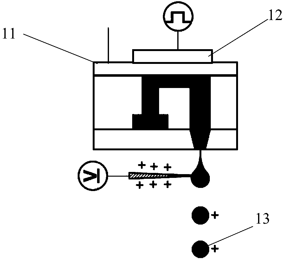
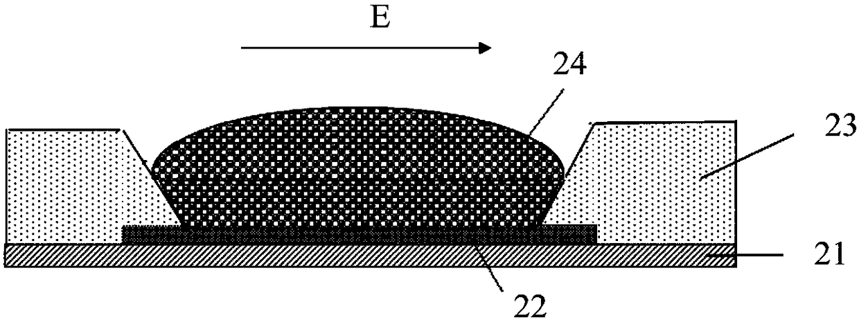
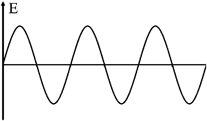
[0037] The embodiments of the present invention aim at the fact that most of the ink solutes used in printing display devices in the prior art are π-conjugated compounds, which are easy to gather due to π-π stacking, resulting in an increase in the surface roughness of the formed thin film functional layer, which seriously limits the display. To solve the problem of improving device efficiency, light color, and lifespan, a film forming method, a display substrate and its manufacturing method, and a display device are provided, which can improve the film morphology of the printed film, thereby improving the performance of the display device.

[0038] The embodiment of the present invention provides a film forming method, comprising:

[...


PUM


Abstract

The invention provides a film forming method, a display substrate, a manufacture method thereof and a display device, and belongs to the technical field of display. The film forming method comprises that an area to form of a film of a substrate is printed with live-line liquid drops of ink in an ink-jet way; and in the ink drying process of the area to form of the film, an electric field is actedon the area, so that the live-line ink is oscillated. According to technical schemes of the invention, the appearance of the film formed by printing can be improved, and performance of the display device is improved.

Description

technical field [0001] The present invention relates to the field of display technology, in particular to a film forming method, a display substrate and a manufacturing method thereof, and a display device. Background technique [0002] Organic Light Emitting Display (OLED) has self-illumination, low driving voltage, high luminous efficiency, short response time, high definition and contrast, wide viewing angle, wide operating temperature range, and can realize flexible display and large-area full-color Display and many other advantages, it is one of the display devices with the most potential for development. [0003] The preparation methods of OLED display devices are mainly divided into two types: vacuum evaporation method and solution method. Compared with the traditional vacuum evaporation method, the solution method, especially the ink-jetting printing method (ink-jetting print) to prepare OLED display devices can greatly improve the utilization rate of materials and ...

Claims


Application Information

Patent Timeline
Patent Type & Authority Applications(China)
IPC IPC(8): H01L51/00H01L51/56
CPCH10K71/135H10K71/00
Inventor 范招康彭锐
Owner BOE TECH GRP CO LTD
Why Eureka
Try Eureka