NO2 chemical resistance type gas sensor and preparation method thereof
A gas sensor and resistive technology, applied in the field of NO2 chemical resistive gas sensor and its preparation, can solve the problems of poor response, slow response, low sensitivity, etc., and achieve high response sensitivity, fast response and recovery speed, and improved sensitivity. Effect
- Summary
- Abstract
- Description
- Claims
- Application Information
AI Technical Summary
Problems solved by technology
Method used
Image
Examples
Embodiment 1
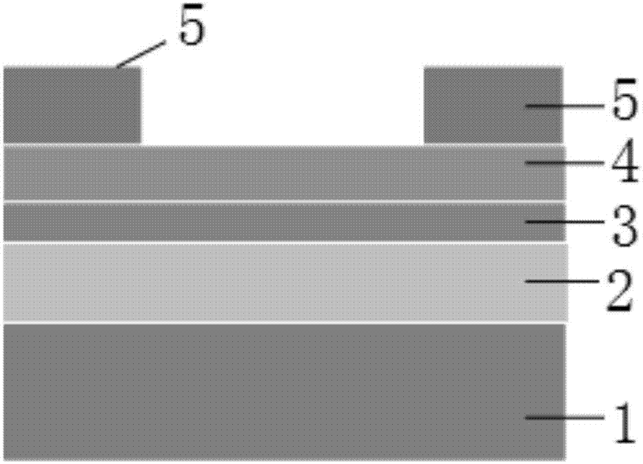
[0039] figure 1 Is the present invention NO 2 Schematic diagram of the structure of a chemical resistive gas sensor, including a substrate 1, an insulating layer 2, a surface modification layer 3, an active sensitive layer 4, and a source-drain electrode 5 arranged in sequence from bottom to top. The material of the insulating layer 2 is silicon oxide, and the surface modification layer The material of layer 3 is an amino-terminated silane compound, and the molecular formula of the amino-terminated silane compound is H 2 N-(CH 2 )3 -Si(OCH 3 ) 3 , the material of the active sensitive layer 4 is TIPS-pentacene. Its preparation method is as follows:
[0040] Select a heavily doped n-type silicon wafer as the substrate 1, which contains 300nm thermally oxidized silicon dioxide (insulating layer 2), and sonicate the substrate 1 in acetone, ethanol, and ultrapure water for ten minutes each to remove surface impurities , and then placed in the volume ratio = 3:7 H 2 o 2 and ...
Embodiment 2
[0044] This example provides a NO 2 Schematic diagram of the structure of a chemical resistive gas sensor, including a substrate 1, an insulating layer 2, a surface modification layer 3, an active sensitive layer 4, and a source-drain electrode 5 arranged in sequence from bottom to top. The material of the insulating layer 2 is silicon oxide, and the surface modification layer The material of layer 3 is an amino-terminated silane compound, and the molecular formula of the amino-terminated silane compound is H 2 N-(CH 2 ) 8 -Si(OCH 3 ) 3 , the active sensitive layer 4 is made of rubrene. Its preparation method is as follows:
[0045] Select a heavily doped n-type silicon wafer as the substrate 1, which contains 300nm thermally oxidized silicon dioxide (insulating layer 2), and sonicate the substrate 1 in acetone, ethanol, and ultrapure water for ten minutes each to remove surface impurities , and then placed in the volume ratio = 3:7 H 2 o 2 and H 2 SO 4 Boil in the m...
Embodiment 3
[0048] This example provides a NO 2 Schematic diagram of the structure of a chemical resistive gas sensor, including a substrate 1, an insulating layer 2, a surface modification layer 3, an active sensitive layer 4, and a source-drain electrode 5 arranged in sequence from bottom to top. The material of the insulating layer 2 is silicon oxide, and the surface modification layer The material of layer 3 is an amino-terminated silane compound, and the molecular formula of the amino-terminated silane compound is H 2 N-(CH 2 ) 3 -Si(OCH 2 CH 3 ) 3 , namely H 2 N-(CH 2 ) 3 -Si(OC 2 h 5 ) 3 , the active sensitive layer 4 is made of vanadyl phthalocyanine. Its preparation method is as follows:
[0049] Select a heavily doped n-type silicon wafer as the substrate 1, which contains 300nm thermally oxidized silicon dioxide (insulating layer 2), and sonicate the substrate 1 in acetone, ethanol, and ultrapure water for ten minutes each to remove surface impurities , and then pl...
PUM
| Property | Measurement | Unit |
|---|---|---|
| thickness | aaaaa | aaaaa |
| thickness | aaaaa | aaaaa |
| thickness | aaaaa | aaaaa |
Abstract
Description
Claims
Application Information


