Preparation method of thin film and light emitting diode

A light-emitting diode and thin-film technology, which is applied in semiconductor/solid-state device manufacturing, electrical components, electric solid-state devices, etc., can solve the problem of unbalanced hole transmission efficiency and electron transmission rate of light-emitting diodes, so as to improve photoelectric performance and working life , Improve the interface contact performance and reduce the effect of interface resistance

Pending Publication Date: 2022-03-18
TCL CORPORATION
View PDF0 Cites 0 Cited by
  • Summary
  • Abstract
  • Description
  • Claims
  • Application Information

AI Technical Summary

Problems solved by technology

[0005] The purpose of this application is to provide a method for preparing a thin film and a light-emitting diode, aiming to solve the problem of the imbalance between the hole transport efficiency and the electron transport rate of the existing light-emitting diodes

Method used


Image

  • Preparation method of thin film and light emitting diode
  • Preparation method of thin film and light emitting diode
  • Preparation method of thin film and light emitting diode

Examples


preparation example Construction

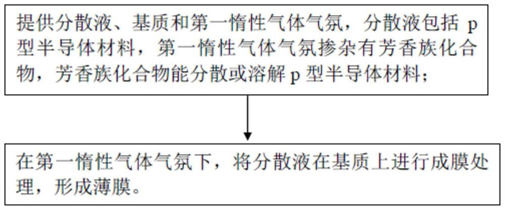
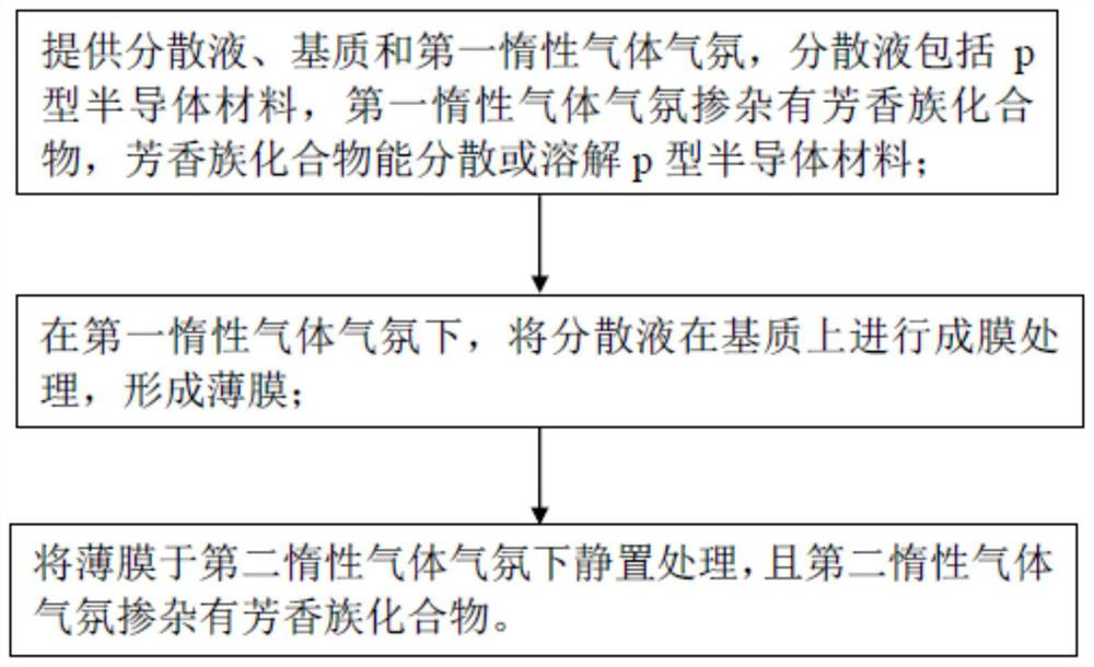
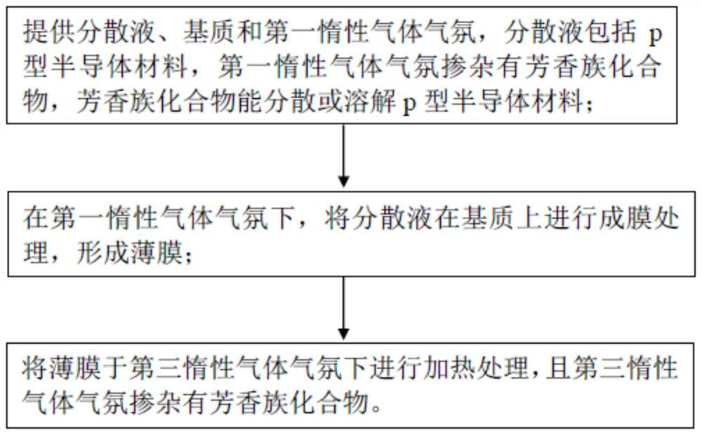
[0032] Such as figure 1 As shown, the embodiment of the present application provides a method for preparing a thin film, comprising the following steps:

[0033] S01. Provide a dispersion liquid, a matrix, and a first inert gas atmosphere, the dispersion liquid includes a p-type semiconductor material, the first inert gas atmosphere is doped with an aromatic compound, and the aromatic compound can disperse or dissolve the p-type semiconductor material;

[0034] S02. Under the first inert gas atmosphere, perform film-forming treatment on the substrate to form a thin film.

[0035] In the method for preparing a thin film provided in an embodiment of the present application, a dispersion liquid comprising a p-type semiconductor material is formed into a film under a first inert gas atmosphere, and the first inert gas atmosphere is doped with an aromatic substance capable of dispersing or dissolving a p-type semiconductor material. A group of compounds, so that in the process of ...

Embodiment 1

[0068] This embodiment provides a top-emitting positive quantum dot light-emitting diode, and its preparation method includes:

[0069] (1) On the ITO substrate, spin-coat PEDOT:PSS at a speed of 5000 for 30 seconds, then heat at 150°C for 15 minutes;

[0070] (2) Doping gaseous chlorobenzene in a glove box environment full of Ar gas atmosphere, and making the volume concentration of gaseous chlorobenzene be 0.5%, then putting the device prepared in step (1) into the glove box;

[0071] (3) Spin-coat TFB (8mg / mL) on the PEDOT:PSS layer at a speed of 3000 for 30 seconds, then heat at 80°C for 10 minutes;

[0072] (4) Put the device prepared in step (3) into a vacuum container, and then replace the gas atmosphere in the glove box with an Ar atmosphere;

[0073] (5) Spin-coat quantum dots (20mg / mL) on the TFB layer at a speed of 2000 for 30 seconds;

[0074] (6) Spin-coat ZnO (30mg / mL) on the quantum dot layer at a speed of 3000 for 30 seconds, then heat at 80°C for 30 minutes;...

Embodiment 2

[0078] This embodiment provides a top-emitting upright quantum dot light-emitting diode, the preparation method of which is basically the same as that of Embodiment 1, the difference is that after heating at 80°C for 10 minutes in step (3), the device is put into an airtight container Standing for 50min, and the atmosphere environment in the airtight container is Ar atmosphere (volume concentration is 95%) and gaseous chlorobenzene (volume concentration 5%), such as Figure 7 shown.


PUM

PropertyMeasurementUnit
diameteraaaaaaaaaa
thicknessaaaaaaaaaa
thicknessaaaaaaaaaa

Abstract

The invention relates to the technical field of display, and provides a preparation method of a thin film and a light emitting diode. The preparation method of the thin film comprises the steps that dispersion liquid, a matrix and a first inert gas atmosphere are provided, the dispersion liquid comprises a p-type semiconductor material, the first inert gas atmosphere is doped with an aromatic compound, and the aromatic compound can disperse or dissolve the p-type semiconductor material; and performing film forming treatment on the dispersion liquid on a substrate in a first inert gas atmosphere to form a thin film. The thin film prepared by the method has a flat and compact surface, and when the thin film is applied to a hole function layer of a light-emitting diode, the thin film morphology of the hole function layer can be improved, and the interface resistance of the hole function layer and a light-emitting layer can be reduced, so that the hole transmission efficiency of a device is improved, and the hole transmission efficiency and electron transmission efficiency of the device are effectively balanced; and the photoelectric property and the service life of the device are improved.

Description

technical field [0001] The present application belongs to the field of display technology, and in particular relates to a thin film preparation method and a light emitting diode. Background technique [0002] QLED (Quantum Dots Light-Emitting Diode, Quantum Dot Light-Emitting Diode), is an emerging display device, the structure is similar to OLED (Organic Light-Emitting Diode, Organic Light-Emitting Display), that is, it mainly consists of a hole transport layer, a light-emitting layer and Sandwich structure composed of electron transport layer. This is a new technology between liquid crystal and OLED. The core technology of QLED is "Quantum Dot (quantum dot)". Atoms make up. As early as 1983, scientists at Bell Laboratories in the United States conducted in-depth research on it, and a few years later, physicist Mark Reed of Yale University officially named it "quantum dots". This substance has a very special property: when the quantum dot is stimulated by light, it will ...

Claims


Application Information

Patent Timeline
Patent Type & Authority Applications(China)
IPC IPC(8): H01L51/56H01L51/50
CPCH10K71/15H10K71/12H10K50/155
Inventor 敖资通严怡然杨帆赖学森洪佳婷张建新
Owner TCL CORPORATION
Why Eureka
Try Eureka