A protection device for power components and its manufacturing method
A technology for protecting devices and power components, applied in semiconductor/solid-state device manufacturing, electrical components, semiconductor devices, etc., can solve the problems of large device area and low surge resistance, and improve device performance, reduce area, reduce The effect of production costs
- Summary
- Abstract
- Description
- Claims
- Application Information
AI Technical Summary
Problems solved by technology
Method used
Image
Examples
Embodiment 1
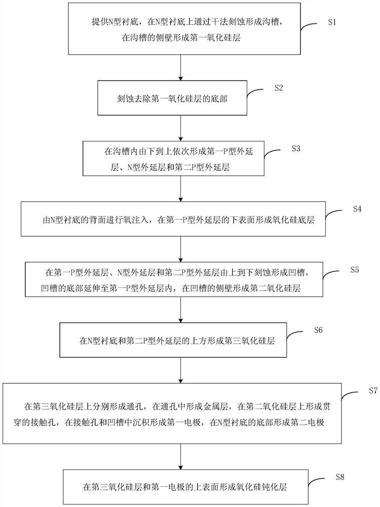
[0038] see figure 1 , a flowchart of a method for manufacturing a protection device for a power element provided by an embodiment of the present invention. A method for manufacturing a protection device for a power element provided by an embodiment of the present invention includes the following steps:
[0039]Step 1: An N-type substrate 100 is provided, a trench is formed on the N-type substrate by dry etching, and a first silicon oxide layer 200 is formed on the sidewall of the trench. see figure 2 , a product schematic diagram of Step 1 in the method for manufacturing a protection device for a power element provided in an embodiment of the present invention.
[0040] Step 2: Etching and removing the bottom of the first silicon oxide layer. see image 3 , a product schematic diagram of Step 2 in the method for manufacturing a protection device for a power element provided in an embodiment of the present invention.
[0041] Step 3: Form a first P-type epitaxial layer 51...
Embodiment 2
[0052] An embodiment of the present invention provides a protection device for a power element. The protection device for a power element is prepared according to the above method for manufacturing a protection device for a power element, and includes: an N-type substrate 100, a first silicon oxide layer 200, and a silicon oxide bottom layer 210, the second silicon oxide layer 300, the third silicon oxide layer 400, the first P-type epitaxial layer 510, the second P-type epitaxial layer 520, the N-type epitaxial layer 530, the metal layer 600, the first electrode 700, and the second electrode 800 and silicon oxide passivation layer 900. see Figure 9 , in the manufacturing method of the power element protection device provided in the above embodiment, the product in the product schematic diagram in Step 8 is a structural schematic diagram of the power element protection device provided by the embodiment of the present invention.
[0053] Wherein, the first silicon oxide layer...
PUM
 Abstract
Description
Claims
Application Information
 - R&D
- Intellectual Property
- Life Sciences
- Materials
- Tech Scout
- Unparalleled Data Quality
- Higher Quality Content
- 60% Fewer Hallucinations
Browse by: Latest US Patents, China's latest patents, Technical Efficacy Thesaurus, Application Domain, Technology Topic, Popular Technical Reports.
© 2025 PatSnap. All rights reserved.Legal|Privacy policy|Modern Slavery Act Transparency Statement|Sitemap|About US| Contact US: help@patsnap.com


